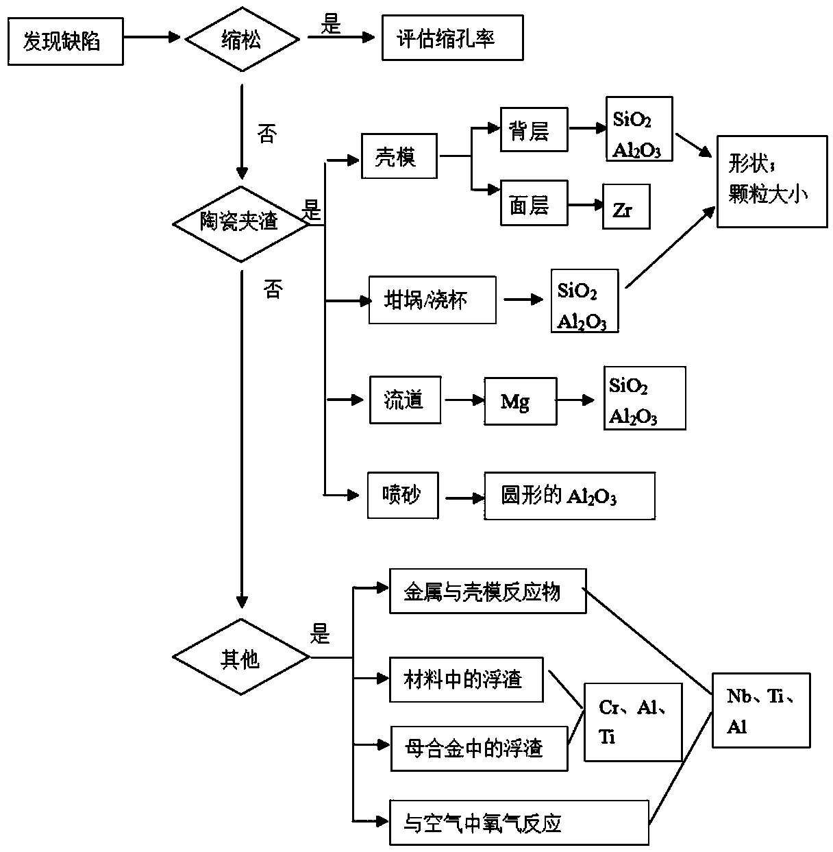
Method for analyzing defect type through scanning electron microscope and microscope
A technology of scanning electron microscopy and defect types, which is applied in the direction of analyzing materials, using wave/particle radiation for material analysis, testing metal components, etc., and can solve problems such as inaccurate determination and inability to find solutions
- Summary
- Abstract
- Description
- Claims
- Application Information
AI Technical Summary
Problems solved by technology
Method used
Image
Examples
Embodiment
[0056] 1. Preliminary judgment is made on the surface defect of the casting, the defect position is displayed with fluorescence, and the defect position is made into a gold image, such as Figure 8 ;
[0057] 2. Use a scanning electron microscope to observe the tissue morphology at 50-1000 times
[0058] 1) Observe its morphological structure: such as Figure 9 , which has no fixed shape and rough edges, and is preliminarily determined to be oxidized slag inclusions;
[0059] 2) if Figure 10 , it can be found that the composition of the defect area is different from that of the base metal, which is in line with the characteristics of oxidized slag inclusions;
[0060] 3) Surface scanning is enriched at the same position, such as Figure 11 As shown, the defect area mainly contains Al and O elements, and more Cr and Nb elements are also detected in the defect area. The detected elements and percentages are shown in the following table:
[0061]
[0062] 3. Conclusion: Th...
PUM
 Abstract
Description
Claims
Application Information


