Three-dimensional memory and method of forming the same

A memory and three-dimensional technology, applied in the direction of semiconductor devices, electric solid-state devices, electrical components, etc., can solve the problems of complex manufacturing process and high manufacturing cost of three-dimensional memory, reduce the number and number of etching times, improve utilization rate, and simplify manufacturing The effect of craft

Active Publication Date: 2022-07-12
YANGTZE MEMORY TECH CO LTD
View PDF4 Cites 0 Cited by
  • Summary
  • Abstract
  • Description
  • Claims
  • Application Information

AI Technical Summary

Problems solved by technology

[0005] The invention provides a three-dimensional memory and its forming method, which are used to solve the problems of complicated manufacturing process and high manufacturing cost of the existing three-dimensional memory

Method used


Image

  • Three-dimensional memory and method of forming the same
  • Three-dimensional memory and method of forming the same
  • Three-dimensional memory and method of forming the same

Examples


Embodiment Construction

[0040] The specific embodiments of the three-dimensional memory provided by the present invention and the method for forming the same will be described in detail below with reference to the accompanying drawings.

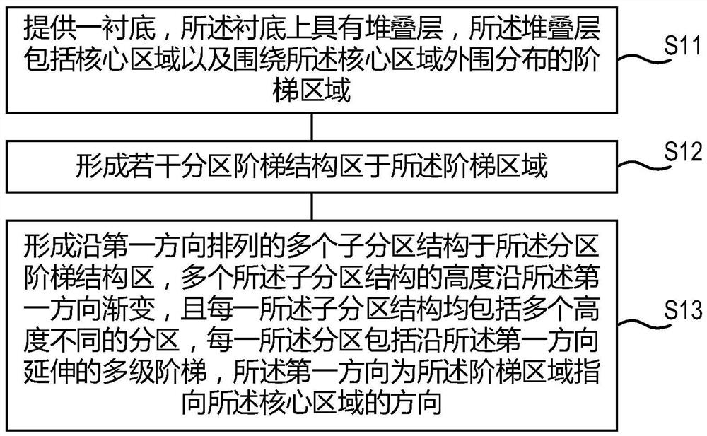
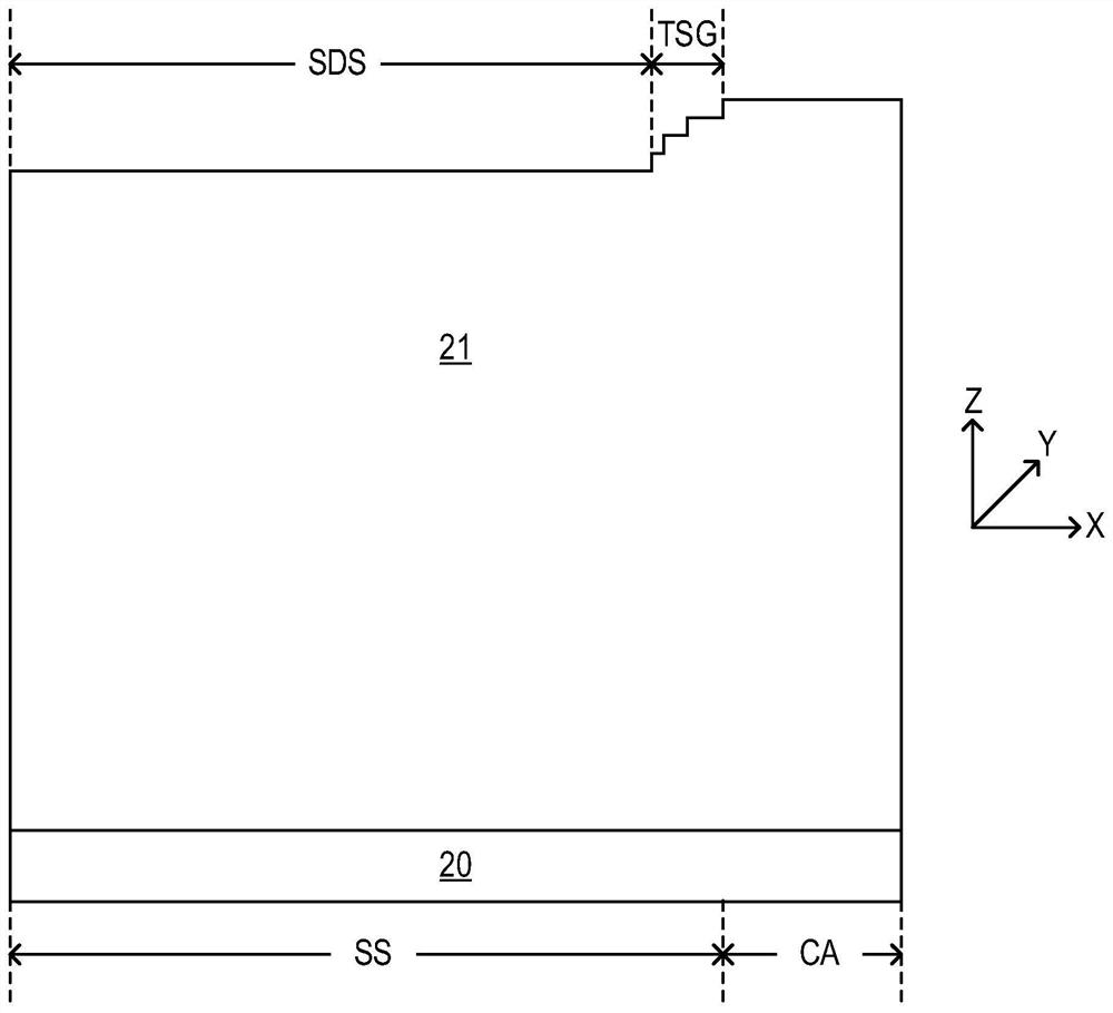
[0041] A three-dimensional memory typically includes a substrate and stacked layers on the substrate, the stacked layers including a core region and a stepped region disposed around the core region. The core area is used for information storage; the stepped area is located at the end of the stack layer, and is used for transmitting control information to the core area, so as to realize the reading and writing of information in the core area.

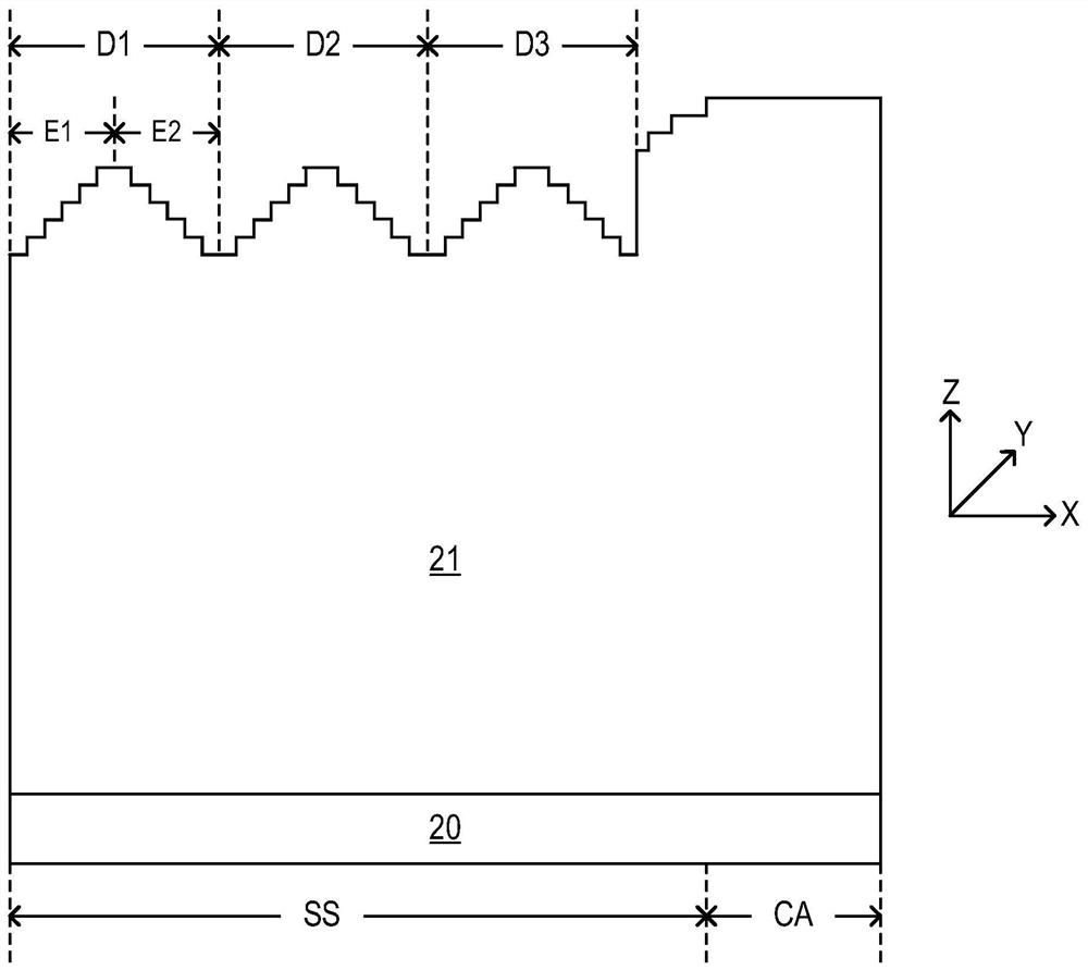
[0042] The traditional stepped area is a one-way stepped structure. However, as the number of stacked layers in 3D memory continues to increase, the unidirectional stepped structure leads to an increase in the area of ​​the stepped region and a dramatic increase in the manufacturing cost. Based on this, the Staircase Divide S...


PUM


Abstract

The present invention relates to the technical field of semiconductor manufacturing, and in particular, to a three-dimensional memory and a method for forming the same. The method for forming the three-dimensional memory includes the following steps: providing a substrate with a stack layer on the substrate, the stack layer including a core region and a stepped region distributed around the periphery of the core region; forming a plurality of partitioned stepped structure regions in the stepped area; a plurality of sub-partition structures arranged along a first direction are formed in the sub-division stepped structure area, and the heights of the plurality of the sub-partition structures are gradually changed along the first direction, and the first direction is the The stepped area points in the direction of the core area. The invention can reduce the number of masks and the times of etching, thereby simplifying the manufacturing process of the three-dimensional memory and reducing the manufacturing cost of the three-dimensional memory.

Description

technical field [0001] The present invention relates to the technical field of semiconductor manufacturing, and in particular, to a three-dimensional memory and a method for forming the same. Background technique [0002] With the development of planar flash memory, the production process of semiconductors has made great progress. However, in recent years, the development of planar flash memory has encountered various challenges: physical limits, existing development technology limits, and storage electron density limits. In this context, in order to solve the difficulties encountered by planar flash memory and pursue lower production costs per unit of memory cells, various three-dimensional (3D) flash memory structures have emerged, such as 3D NOR (3D or non) flash memory and 3D NAND (3D and not) flash memory. [0003] Among them, 3D NAND memory is based on its small size and large capacity, and the high integration of storage cells using three-dimensional mode layer-by-l...

Claims


Application Information

Patent Timeline
Patent Type & Authority Patents(China)
IPC IPC(8): H01L27/11578
CPCH10B43/20
Inventor 李治昊夏志良周文犀张帜张中
Owner YANGTZE MEMORY TECH CO LTD
Why Eureka
Try Eureka