
LED lamp panel and preparation method thereof, and display device

A technology of LED light boards and LED chips, which is applied in the direction of electrical components, electric solid devices, circuits, etc., can solve the problems of unfavorable thinning of liquid crystal display devices, large LED thickness, and increased light mixing distance, so as to achieve the development of light and thin, High contrast, reduce the effect of light mixing distance

Inactive Publication Date: 2019-12-03
HISENSE VISUAL TECH CO LTD
View PDF9 Cites 2 Cited by
  • Summary
  • Abstract
  • Description
  • Claims
  • Application Information

AI Technical Summary

Problems solved by technology

[0004] At present, the size of the LED used in the LED light source 02 is usually not less than 3mm, the light is concentrated, and it is easy to cause uneven light mixing
In order to ensure uniform light mixing, it is usually necessary to increase the backlight film, which will increase the light mixing distance; and the thickness of the LED is relatively large, which increases the thickness of the LED backlight module to a certain extent, which is not conducive to the development of light and thin liquid crystal display devices

Method used


Image

  • LED lamp panel and preparation method thereof, and display device
  • LED lamp panel and preparation method thereof, and display device
  • LED lamp panel and preparation method thereof, and display device

Examples


Embodiment Construction

[0023] In order to make the purpose, technical solution and advantages of the present application clearer, the present application will be further described in detail below in conjunction with the accompanying drawings and embodiments. It should be understood that the specific embodiments described here are only used to explain the present application, and are not intended to limit the present application.

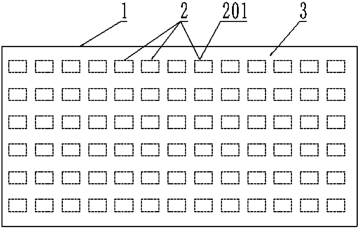
[0024] figure 2 The front view of the LED lamp panel provided by the embodiment of this application; image 3 A schematic cross-sectional structure diagram of an LED lamp panel provided in an embodiment of the present application. attached by figure 2 and 3 As shown, the LED light board provided by the embodiment of the present application includes a circuit board 1; an LED chip array 2 arranged on the circuit board 1, the LED chip array 2 is in electrical communication with the circuit board 1, and the LED chip The array 2 includes several LED chips 201 ; the LED la...


PUM


Abstract

The invention provides an LED lamp panel. The LED lamp panel comprises: a circuit board; a LED chip array arranged on the circuit board and comprising a plurality of LED chips, wherein the LED chip array is electrically connected with the circuit board; and a packaging layer, wherein the packaging layer covers the LED chip array, wherein the packaging layer comprises a packaging adhesive. Based onthe LED lamp panel provided by the invention, the invention further provides a preparation method of the LED lamp panel and a display device. According to the LED lamp panel and the preparation method thereof and the display device, the LED lamp panel is high in light emitting efficiency, good in heat dissipation, small in LED chip size and uniform in light emitting, a thick and heavy traditionaltelevision backlight diaphragm can be removed, the light mixing distance is reduced, the ultrathin module design is achieved, and light and thin development of a backlight module is facilitated.

Description

technical field [0001] The present application relates to the technical field of liquid crystal televisions, in particular to an LED lamp panel, a preparation method thereof and a display device. Background technique [0002] A liquid crystal display device currently on the market usually consists of two parts: a liquid crystal display panel and a backlight module. Since the liquid crystal display panel itself does not emit light, it needs the light generated by the backlight module to display images normally, so the backlight module becomes an integral part of the liquid crystal display. [0003] In the backlight module, the backlight board is the core component used to provide the light source. In the prior art, the backlight board is usually a light bar with a strip structure, including a strip circuit board and a light source arranged on the circuit board, such as Set LED (Light-Emitting Diode, light-emitting diode) on PCB (Printed Circuit Board, printed circuit board)....

Claims


Application Information

Patent Timeline
Patent Type & Authority Applications(China)
IPC IPC(8): H01L33/48H01L33/52H01L25/075
CPCH01L25/0753H01L33/486H01L33/52H01L2933/0033H01L2933/005
Inventor 刘振国宋志成曹建伟
Owner HISENSE VISUAL TECH CO LTD
Learn More