Supercharge Your Innovation With Domain-Expert AI Agents!

Silicon wafer manufacturing method and device

A manufacturing method and a manufacturing device technology, which are applied in the field of silicon wafer manufacturing methods and manufacturing devices, and can solve problems such as adverse effects on the function of electronic components

Pending Publication Date: 2019-12-13
DATONG XINCHENG NEW MATERIAL CO LTD
View PDF0 Cites 0 Cited by
  • Summary
  • Abstract
  • Description
  • Claims
  • Application Information

AI Technical Summary

Problems solved by technology

If preventive measures are not taken: Defects remain on the wafer surface which can adversely affect the functionality of the electronic components on the wafer surface

Method used


Image

  • Silicon wafer manufacturing method and device
  • Silicon wafer manufacturing method and device
  • Silicon wafer manufacturing method and device

Examples


Embodiment Construction

[0027] In order to enable those skilled in the art to better understand the technical solutions in the present invention, the technical solutions in the embodiments of the present invention will be clearly and completely described below in conjunction with the drawings in the embodiments of the present invention. Obviously, the described The embodiments are only some of the embodiments of the present invention, not all of them. Based on the embodiments of the present invention, all other embodiments obtained by persons of ordinary skill in the art without making creative efforts shall fall within the protection scope of the present invention.

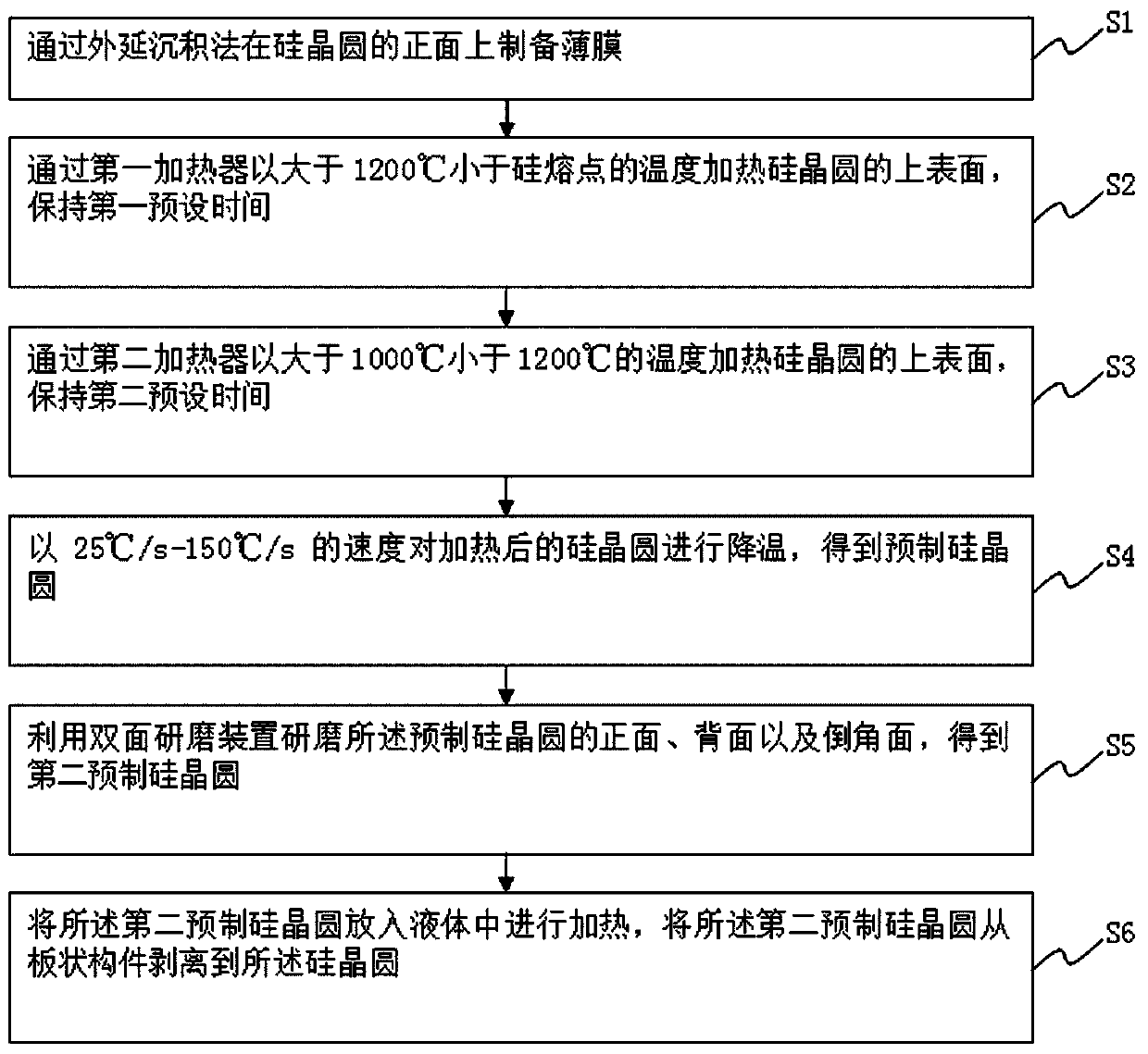
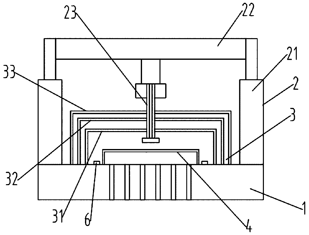
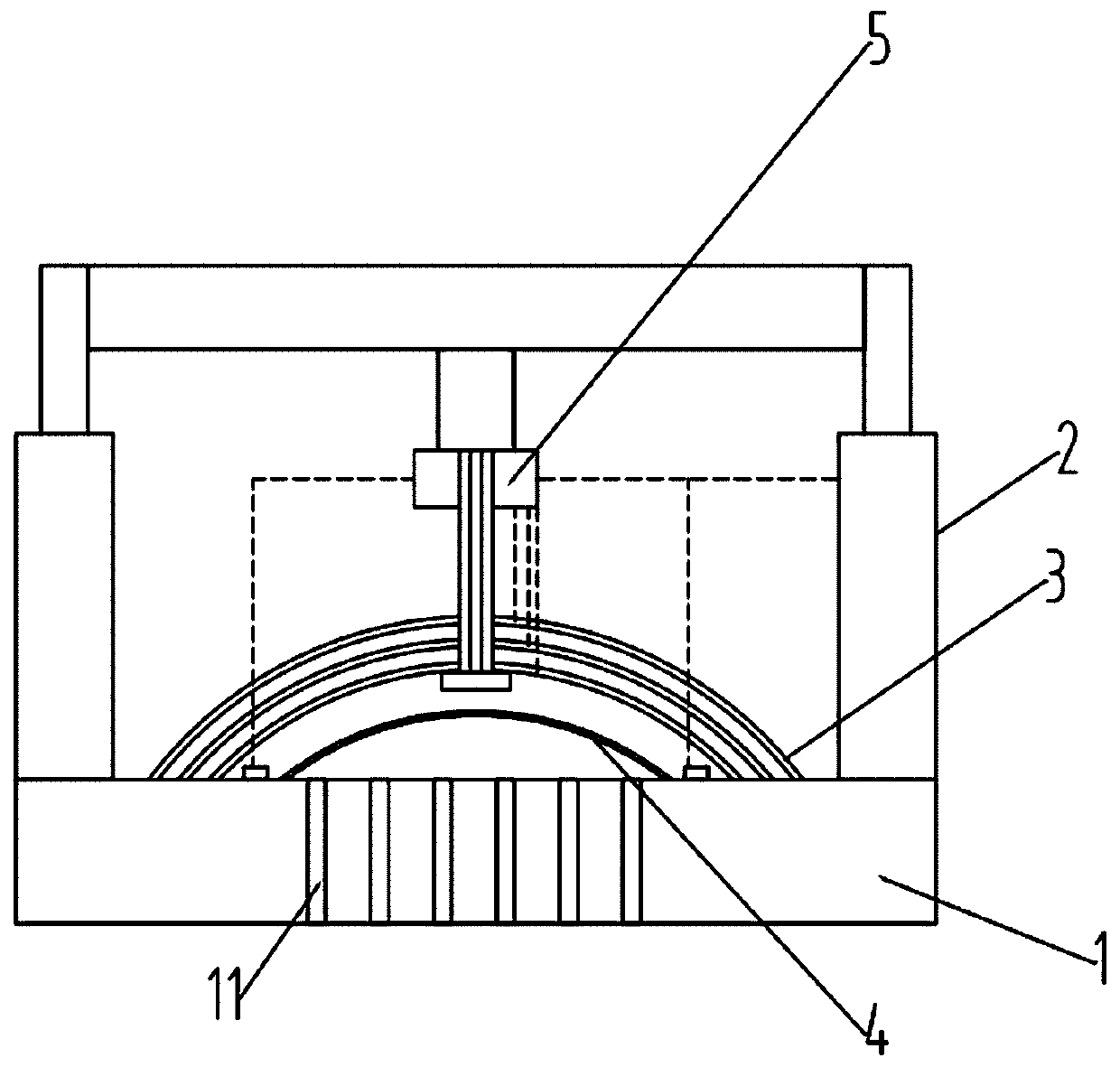
[0028] According to a first aspect of the present disclosure, a silicon wafer manufacturing method, such as figure 1 Shown, described silicon wafer manufacturing method comprises the following steps:

[0029] S1: Prepare a thin film on the front side of the silicon wafer by epitaxial deposition;

[0030] S2: using the first heater to ...


PUM

PropertyMeasurementUnit
diameteraaaaaaaaaa

Abstract

The invention provides a silicon wafer manufacturing method and device. The silicon wafer manufacturing method comprises the steps of firstly, preparing a thin film on the front surface of a silicon wafer through an epitaxial deposition method, heating the upper surface of the silicon wafer at a temperature which is greater than 1200 DEG C and less than a silicon melting point through a first heater, heating the upper surface of the silicon wafer at a temperature which is greater than 1000 DEG C and less than 1200 DEG C through a second heater, and cooling the heated silicon wafer to obtain aprefabricated silicon wafer; grinding the front surface, the back surface and the chamfered surface of the prefabricated silicon wafer by using a double-sided grinding device to obtain a second prefabricated silicon wafer; and putting the second prefabricated silicon wafer into the liquid for heating, and stripping the second prefabricated silicon wafer from the plate-shaped component to obtain the silicon wafer. According to the silicon wafer manufacturing method, annealing treatment is carried out on the surface of the silicon wafer, so that the surface of the silicon wafer is enabled to slowly release stress and be slowly cooled to obtain a stable structure close to an equilibrium state, defects on the surface of the silicon wafer are reduced, and adverse effects of the surface defectson functions of electronic components on the surface of the wafer are reduced.

Description

technical field [0001] The invention relates to the technical field of semiconductor materials, in particular to a silicon wafer manufacturing method and manufacturing device. Background technique [0002] The wafer is silicon element to be purified (99.999%), and then these pure silicon are made into long silicon crystal rods, which become the material of quartz semiconductors for manufacturing integrated circuits. The monocrystalline silicon rod is melted and pulled out, and then cut into thin wafers. In recent years, solar power generation has attracted attention as an energy alternative to petroleum. Since it is desired to reduce the cost of silicon wafers used in large quantities in solar power generation, it is desired to efficiently utilize silicon ingots to manufacture silicon wafers. The method of manufacturing a silicon wafer generally includes the following steps: a bonding step, a slicing step, a rough cleaning and peeling step, a wafer dicing step, a cleaning ...

Claims


Application Information

Patent Timeline
Patent Type & Authority Applications(China)
IPC IPC(8): H01L21/67H01L21/02
CPCH01L21/67098H01L21/02008
Inventor 王振国
Owner DATONG XINCHENG NEW MATERIAL CO LTD
Features
  • R&D
  • Intellectual Property
  • Life Sciences
  • Materials
  • Tech Scout
  • Unparalleled Data Quality
  • Higher Quality Content
  • 60% Fewer Hallucinations
Learn More