Manufacturing method of metal nanowire and semiconductor device and manufacturing method thereof
A technology of metal nanowires and a manufacturing method, which is applied in the fields of semiconductor/solid-state device manufacturing, semiconductor devices, semiconductor/solid-state device components, etc. Equalize the problem to achieve the effect of ensuring performance, high sidewall topography, and high thickness uniformity
- Summary
- Abstract
- Description
- Claims
- Application Information
AI Technical Summary
Problems solved by technology
Method used
Image

Examples
Embodiment Construction
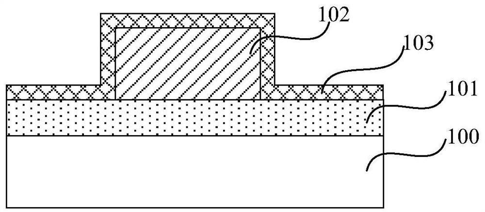
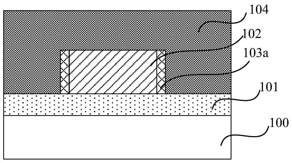
[0051] Please refer to Figure 1A to Figure 1E , a known method of manufacturing a semiconductor device with metal nanowires, comprising the steps of:
[0052] First, please refer to Figure 1A On a semiconductor substrate 100, the bottom anti-reflection layer (for example, SiCN) 101 and the core layer are sequentially covered, and the core layer is patterned through processes such as photoresist coating, exposure, and development to form a patterned core layer. nuclear layer 102;
[0053] Then, please continue to refer to Figure 1A , using a deposition process of materials such as Ru to cover the surface of the patterned core layer 102 and the etching stop layer 101 with a metal layer 103, and the deposition thickness of the metal layer 103 in each region is basically the same;
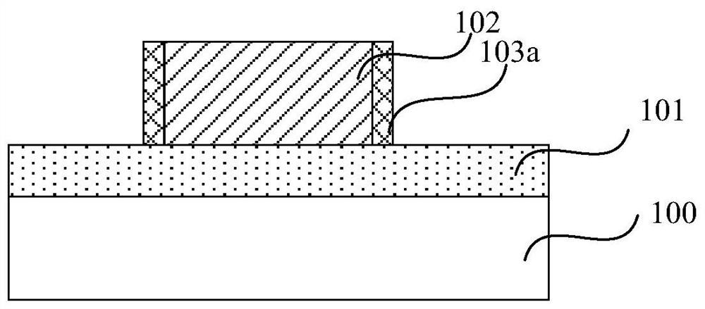
[0054] Next, please refer to Figure 1B , using an anisotropic metal etching process to etch the metal layer until the top surface of the patterned core layer 102 and the top surface of the etch ...
PUM
| Property | Measurement | Unit |
|---|---|---|
| thickness | aaaaa | aaaaa |
| width | aaaaa | aaaaa |
Abstract
Description
Claims
Application Information