Epitaxial growth device and epitaxial growth method

A technology of epitaxial growth and equipment, applied in chemical instruments and methods, crystal growth, single crystal growth, etc., can solve problems such as adjustment, difficult structure, and poor flexibility

Inactive Publication Date: 2019-12-17
ZING SEMICON CORP
View PDF6 Cites 3 Cited by
  • Summary
  • Abstract
  • Description
  • Claims
  • Application Information

AI Technical Summary

Problems solved by technology

However, adjusting the structure of the epitaxial growth device needs to consider the impact on the various functional components of the device, which is relatively

Method used


Image

  • Epitaxial growth device and epitaxial growth method
  • Epitaxial growth device and epitaxial growth method
  • Epitaxial growth device and epitaxial growth method

Examples


Embodiment Construction

[0036] The epitaxial growth equipment and epitaxial growth method of the present invention will be further described in detail below in conjunction with the accompanying drawings and specific embodiments. The advantages and features of the present invention will become clearer from the following description. It should be noted that all the drawings are in very simplified form and use imprecise scales, and are only used to facilitate and clearly illustrate the embodiments of the present invention.

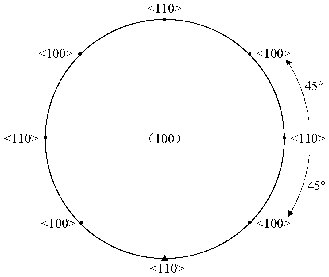
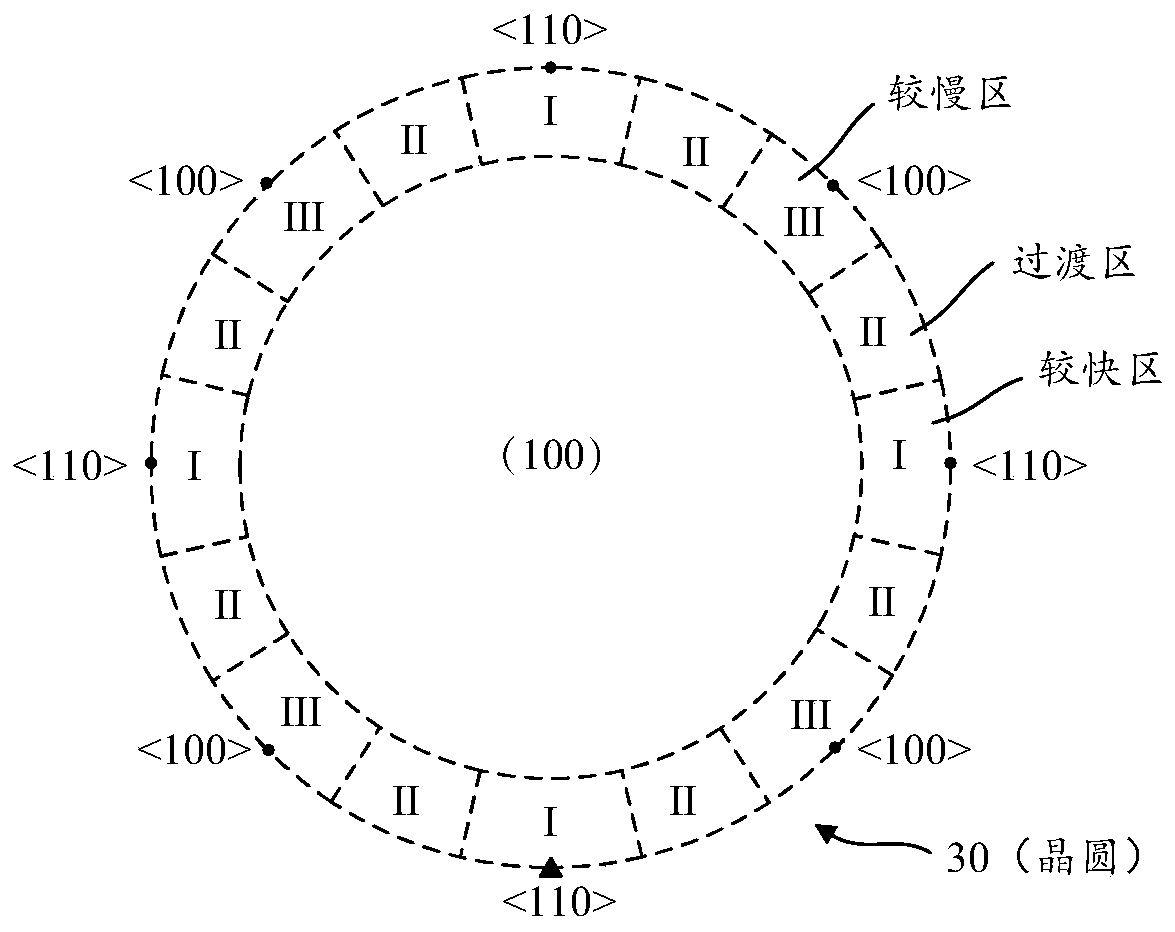
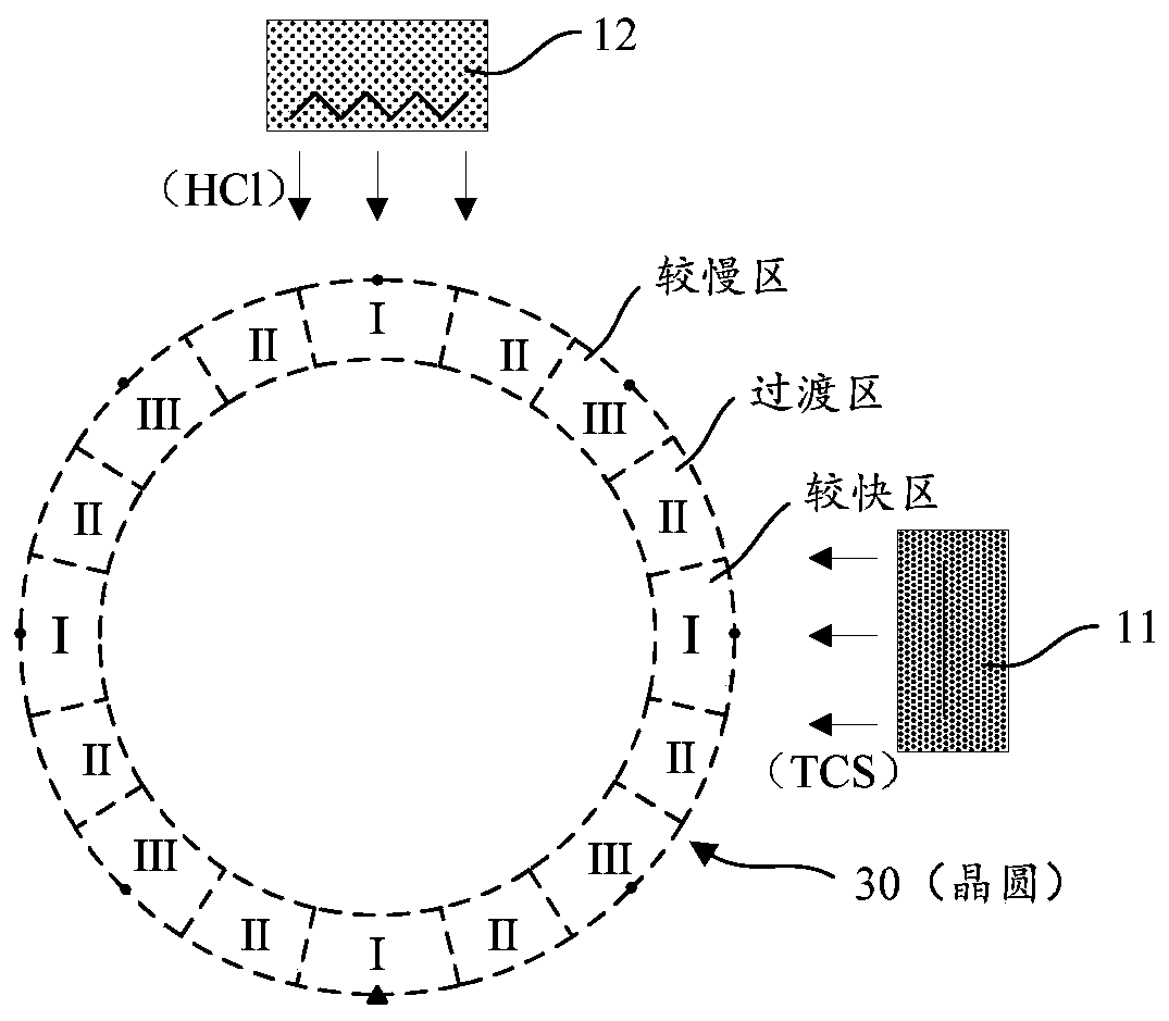
[0037] In the manufacturing process of semiconductor wafers, the semiconductor wafers formed by dicing are usually subjected to grinding steps, such as grinding or lapping, to round the mechanically sensitive edges, then polished and cleaned, and then formed by vapor growth on the upper surface of the wafer in epitaxial growth equipment epitaxial layer.

[0038] In the epitaxial growth process, a semiconductor wafer such as a silicon wafer is placed in an epitaxial growth device to...


PUM


Abstract

The invention provides an epitaxial growth device and an epitaxial growth method. The cavity of the epitaxial growth device is provided with a first air inlet and a second air inlet, wherein the firstair inlet allows a reactive gas used for forming an epitaxial layer on a wafer to enter the cavity, and the second air inlet allows an etching gas used for preventing deposition of the epitaxial layer to enter the cavity; when the edge part of the wafer has a faster area and a slower area with different crystal orientations and the epitaxial layer grows faster in the faster area than in the slower area, along with rotation of the wafer in the epitaxial process, the air inlet rate of the etching gas provided by the second air inlet when the second air inlet rotates past the faster area is higher than that of the etching gas provided by the second air inlet when the second air inlet rotates past the slower area, so that the etching gas has higher removal efficiency for the epitaxial layer of the faster area, the epitaxial growth of the faster area and the slower area can be adjusted, the thickness uniformity of the epitaxial layer is improved, the local straightness is reduced, and thequality of the epitaxial wafer is improved.

Description

technical field [0001] The invention relates to the field of epitaxial growth technology, in particular to an epitaxial growth device and an epitaxial growth method. Background technique [0002] The manufacturing of electronic components has high requirements on the flatness of the upper surface of the semiconductor wafer as the substrate. Now the local flatness SFQR (least squares of the reference of the upper surface of the part) is commonly used to take into account the focusing ability of the stepping device in all areas of the wafer surface square / range) parameters to evaluate. Maximum local flatness SFQR max The value of represents the maximum SFQR value of all electronic components considered on the semiconductor wafer. QUR max The reduction of the value is beneficial to solve the problem of defocusing of the photolithography process that may be encountered in the manufacture of electronic devices, the problem of polishing uniformity in the CMP process, and the pr...

Claims


Application Information

Patent Timeline
IPC IPC(8): C30B25/20C30B25/16C30B25/14C30B29/06
CPCC30B25/20C30B25/165C30B25/14C30B29/06
Inventor 费璐林志鑫曹共柏王华杰董晨华季文明
Owner ZING SEMICON CORP
Why Eureka
Try Eureka