Liquid crystal display panel with switchable wide and narrow viewing angles and liquid crystal display device
A liquid crystal display panel, viewing angle technology, applied in nonlinear optics, instruments, optics, etc., can solve the problems affecting the display effect and anti-peeping effect, and achieve the effect of light and thin power consumption, low power consumption, and improved visual performance
- Summary
- Abstract
- Description
- Claims
- Application Information
AI Technical Summary
Problems solved by technology
Method used
Image
Examples
no. 1 example
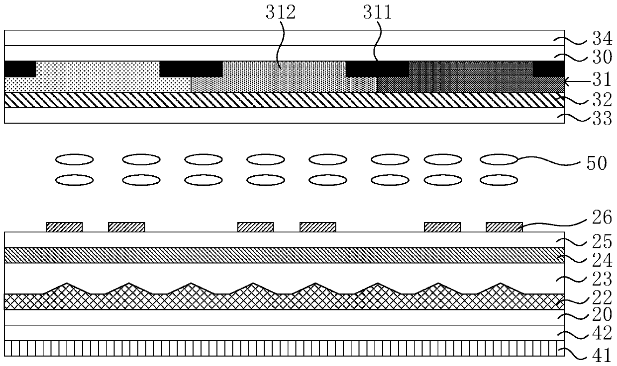
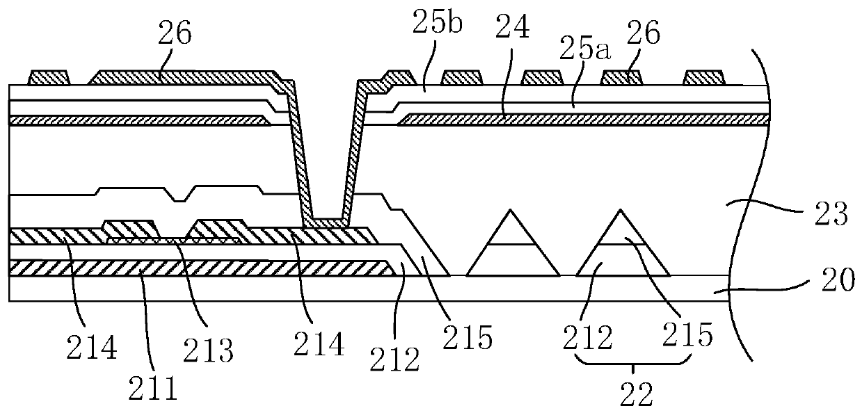
[0038] Please refer to figure 2 , shows a schematic structural view of a liquid crystal display panel with switchable wide and narrow viewing angles according to the first embodiment of the present invention. The liquid crystal display panel includes: a first substrate 20 , a second substrate 30 opposite to the first substrate 20 , and a liquid crystal layer 50 between the first substrate 20 and the second substrate 30 . The side of the first substrate 20 away from the liquid crystal layer 50 is provided with a light collecting film 41, and the first substrate 20 is provided with a prism layer 22 on the side facing the liquid crystal layer 50, and the light collecting film 41 is used to narrow the 20 Light incident on the side far away from the liquid crystal layer 50, transforming the incident light into collimated light or light distributed within a certain angle range (such as 60°) with the vertical direction, so as to avoid whitening of both sides when the liquid crystal ...
no. 2 example
[0053] Please refer to Figure 8 The difference between the liquid crystal display panel with switchable wide and narrow viewing angles of the second embodiment of the present invention and the first embodiment above is that the second common electrode 32 is a patterned structure.
[0054] The second common electrode 32 is arranged corresponding to the black matrix 311, and has a plurality of sensing opening areas TA corresponding to a plurality of pixel openings, that is, the second common electrode 32 is, for example, a strip structure or a grid correspondingly arranged under the black matrix 311. The area on the second substrate 30 correspondingly covered by the second common electrode 32 is the sensing shielding area TB, and the area not correspondingly covered by the second common electrode 32 is the sensing opening area TA. The width of the second common electrode 32 can be narrower than that of the black matrix 311 to reduce the influence on the pixel aperture ratio, an...
PUM
 Abstract
Description
Claims
Application Information


