Artificial nerve synaptic device and preparation method thereof

A technology of synaptic devices and artificial nerves, applied in the field of bionic electronics, can solve problems such as inability to simultaneously realize associative learning-related characteristics, complex circuit structure, and complex input signals

Inactive Publication Date: 2019-12-20
INST OF MICROELECTRONICS CHINESE ACAD OF SCI
View PDF3 Cites 4 Cited by
  • Summary
  • Abstract
  • Description
  • Claims
  • Application Information

AI Technical Summary

Problems solved by technology

[0003] What the present invention aims to solve is the problem that the circuit structure is complicated or the input signal is complex and the releva

Method used


Image

  • Artificial nerve synaptic device and preparation method thereof
  • Artificial nerve synaptic device and preparation method thereof
  • Artificial nerve synaptic device and preparation method thereof

Examples


Example Embodiment

[0039] Example 1

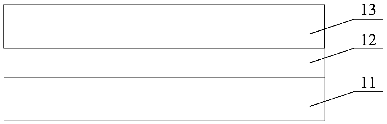
[0040] This embodiment provides an artificial nerve synapse device, figure 1 Schematic diagram of the structure of the artificial nerve synapse device, the artificial nerve synapse device includes a first electrode layer 11, a second electrode layer 13, and a layer disposed between the first electrode layer 11 and the second electrode layer 13. between functional layers 12.

[0041] Specifically, the first electrode layer 11 is used as a bottom electrode, and the material thereof may be an inert conductive material such as Pd, Pt, ITO, W, or Au. Further, the thickness of the first electrode layer 11 is 10 nanometers to 200 nanometers.

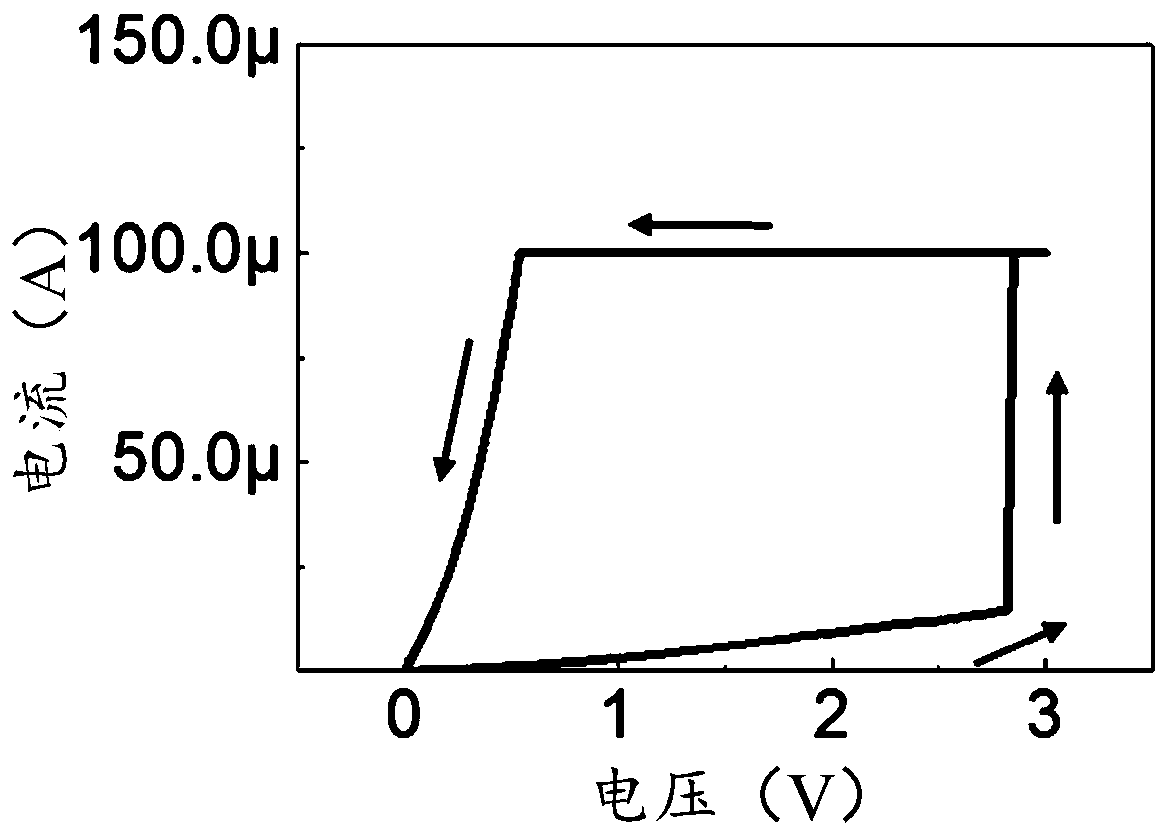
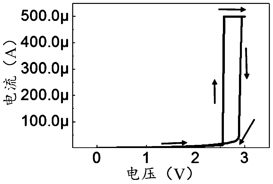
[0042] The resistive switching device prepared based on the material of the functional layer 12 has both unidirectional resistive switching characteristics and bidirectional resistive switching characteristics. Unidirectional resistive characteristics, also known as unipolar resistive behavior, means that resistive behavio...

Example Embodiment

[0048] Example 2

[0049] Based on the same inventive concept, this embodiment provides a method for manufacturing the artificial neural synapse device provided in Embodiment 1 by plane integration, and the manufacturing method for the artificial neural synapse device includes steps S11 to S15.

[0050] S11, providing a semiconductor substrate.

[0051] like Figure 8a As shown, the semiconductor substrate 81 may be a silicon substrate.

[0052] S12, depositing an isolation layer on the surface of the semiconductor substrate.

[0053] like Figure 8b As shown, the isolation layer 82 is deposited on the surface of the semiconductor substrate 81 by chemical vapor deposition or thermal oxidation. The material of the isolation layer 82 can be SiO 2 Or SiN, which can be 100nm to 300nm thick. Of course, the thickness of the isolation layer 82 may also be reduced or increased according to actual process conditions, which is not limited in this embodiment.

[0054] S13, deposit...

Example Embodiment

[0060] Example 3

[0061] Based on the same inventive concept, this embodiment provides a method for vertically integrating the artificial nerve synapse device provided in Embodiment 1, and the method for preparing the artificial nerve synapse device includes steps S21 to S27.

[0062] S21, providing a semiconductor substrate.

[0063] like Figure 9a As shown, the semiconductor substrate 91 may be a silicon substrate.

[0064] S22, depositing a first isolation layer on the surface of the semiconductor substrate.

[0065] like Figure 9b As shown, the first isolation layer 92 is deposited on the surface of the semiconductor substrate 91 by chemical vapor deposition or thermal oxidation. The material of the first isolation layer 92 may be SiO 2 Or SiN, which can be 100nm to 300nm thick. Of course, the thickness of the first isolation layer 92 may also be reduced or increased according to actual process conditions, which is not limited in this embodiment.

[0066] S23, de...


PUM

PropertyMeasurementUnit
Thicknessaaaaaaaaaa
Thicknessaaaaaaaaaa
Thicknessaaaaaaaaaa

Abstract

The invention discloses an artificial nerve synaptic device and a preparation method thereof. The artificial nerve synaptic device comprises a first electrode layer, a second electrode layer and a function layer arranged between the first electrode layer and the second electrode layer. The resistive random access device prepared based on the material of the function layer has a unidirectional resistive random access characteristic and a bidirectional resistive random access characteristic at the same time. According to the artificial neural synaptic device and the preparation method thereof, related characteristics of associative learning and non-associative learning can be realized at the same time, and when the related characteristics of non-associative learning are realized, a three-terminal transistor does not need to be matched, and complex excitation conditions do not need to be provided.

Description

technical field [0001] The invention relates to the technical field of bionic electronics, in particular to an artificial neural synapse device and a preparation method thereof. Background technique [0002] In recent years, the artificial biological nervous system based on the device level is developing into an important branch in the field of artificial intelligence. The artificial synaptic device is a resistance-adjustable device that can adjust the weight of the front and rear neuron circuit connections, and has important applications in the construction of artificial nervous systems. At present, the artificial synaptic devices that can realize the relevant characteristics of non-associative learning, such as the artificial neural synaptic devices that realize sensitive and habitual characteristics, need to cooperate with three-terminal transistors or need to provide complex excitation conditions, so in the realization of non-associative learning. There is a problem tha...

Claims


Application Information

Patent Timeline
IPC IPC(8): H01L45/00
CPCH10N70/20H10N70/011
Inventor 刘琦吴祖恒时拓刘明吕杭炳张续猛
Owner INST OF MICROELECTRONICS CHINESE ACAD OF SCI
Why Eureka
Try Eureka