Back plate, backlight module, display device and preparation method of back plate
A backplane and seed technology, applied in optics, nonlinear optics, instruments, etc., can solve problems such as affecting the shape of thick Cu, collapse of retaining walls, and reduced luminous performance of Mini-LEDs
- Summary
- Abstract
- Description
- Claims
- Application Information
AI Technical Summary
Problems solved by technology
Method used
Image
Examples
Embodiment 1
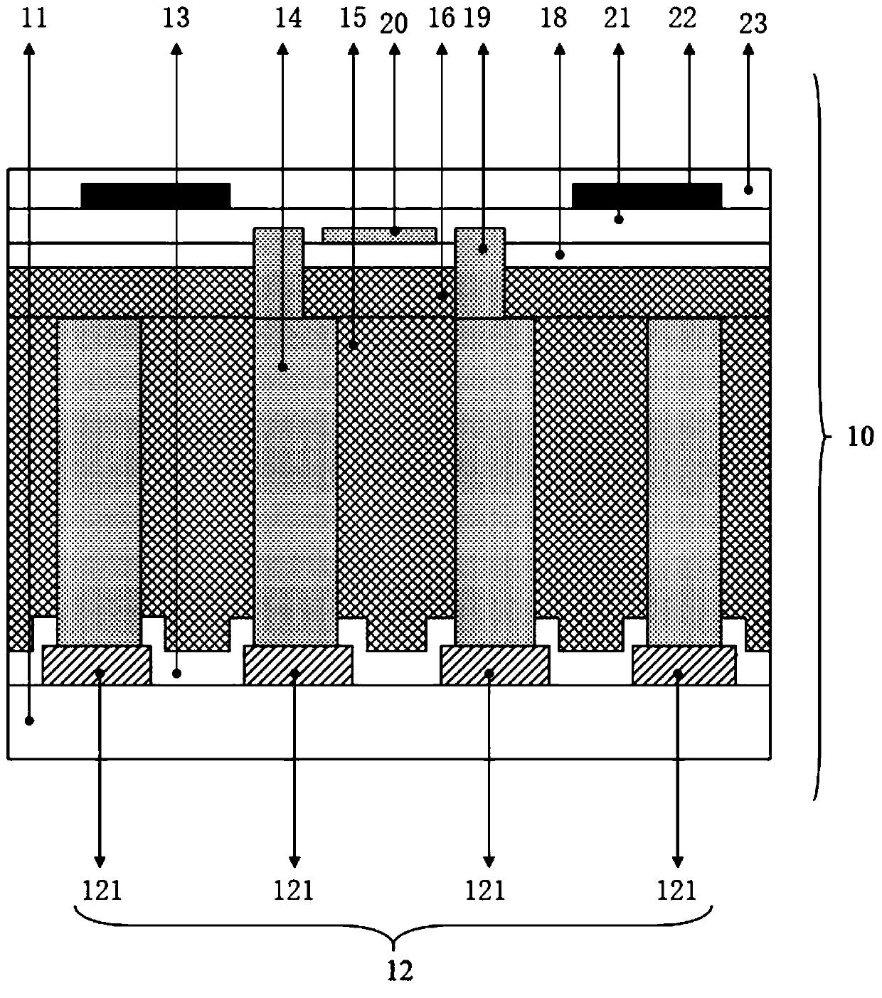
[0051] refer to figure 1 , providing a backplane 10, comprising:
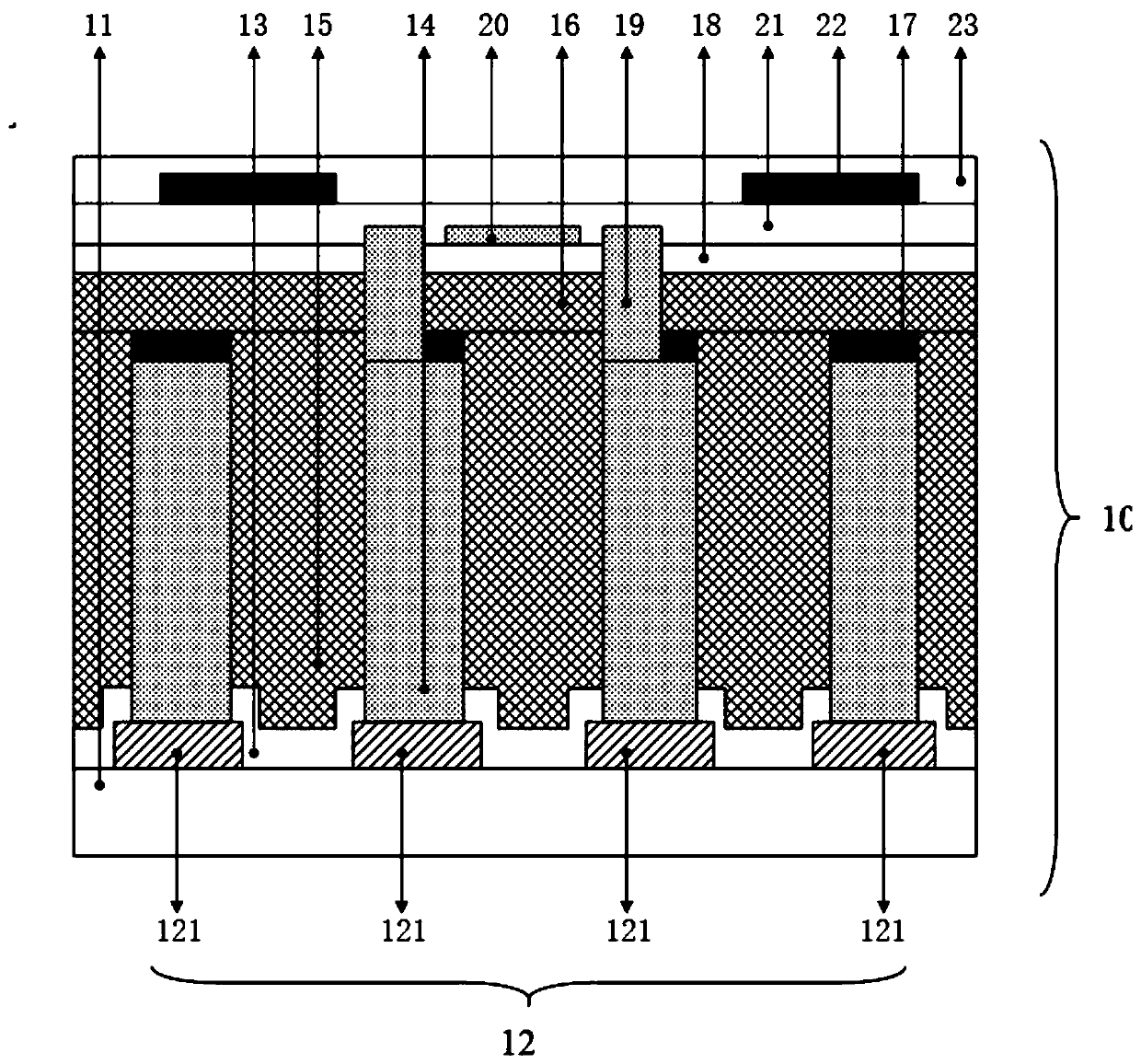
[0052] Substrate 11; seed layer 12, said seed layer 12 includes: a plurality of electrode seeds 121 arranged at intervals on said substrate; protective layer 13, said protective layer 13 is arranged between adjacent electrode seeds 121, and covers all The edge area of the electron seed 121; the electrode block 14, each of the electrode blocks 14 is arranged on the electrode seed 121 between the adjacent protective layers 13, and is located on the side of the electrode seed 121 away from the substrate 11; the filling layer 15 , the filling layer 15 is filled between the electrode blocks 14; the leveling layer 16, the leveling layer 16 covers the filling layer 15 and one of the electrode blocks 14 away from the electrode seeds 121 side.
[0053] In the embodiment of the present invention, the substrate includes: a glass substrate; the material of the seed layer includes: metal copper.
[0054] Among them, the ...
Embodiment 2
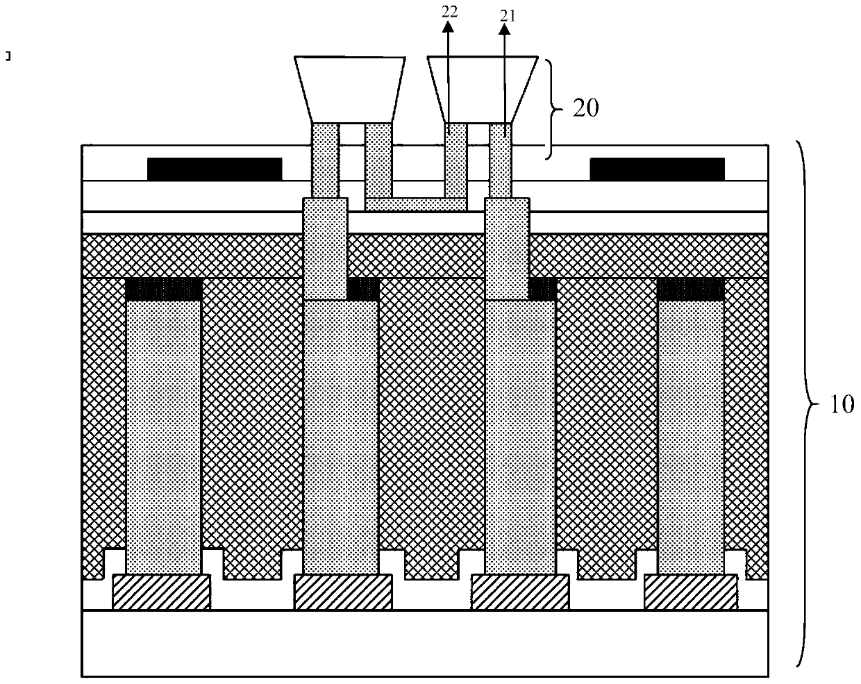
[0074] refer to image 3 The second aspect of the present invention is to provide a backlight module, including the above-mentioned backplane 10 and a plurality of point light sources 20; the point light sources 20 are arranged on one side of the backplane; the point light sources include : the first electrode 21 and the second electrode 22 ; the first electrode 21 is connected to the first connection electrode 19 , and the second electrode 22 is connected to the second connection electrode 20 .
[0075] In the embodiment of the present invention, the point light source includes: a mini-LED, and the first electrode and the second electrode can be positive and negative respectively, and are used to connect a power source to supply power to the mini-LED.
[0076] A third aspect of the present invention is to provide a display device, including the above-mentioned backlight module.
[0077] In an embodiment of the present invention, the backplane includes: a substrate; a seed la...
Embodiment 3
[0079] refer to Figure 4 , the embodiment of the present invention provides a fourth aspect of the present invention to provide a method for preparing a backplane, using the backplane described in any one of the above methods, the method comprising:
[0080] Step 201 , providing a substrate 11 .
[0081] In an embodiment of the present invention, the substrate includes: a glass substrate.
[0082] Step 202 , preparing a seed layer 12 on the substrate 11 ; the seed layer includes: a plurality of electrode seeds 121 arranged at intervals.
[0083] Step 203, coating a protective material on the substrate and the side of the electrode seed facing away from the substrate, and patterning the protective material to obtain a protective layer 13, so that the protective layer is placed on the electrode between the seeds and cover the edge regions of the electron seeds.
[0084] In the embodiment of the present invention, the protection layer is a polymer of inorganic silicon nitride...
PUM
| Property | Measurement | Unit |
|---|---|---|
| thickness | aaaaa | aaaaa |
| thickness | aaaaa | aaaaa |
| thickness | aaaaa | aaaaa |
Abstract
Description
Claims
Application Information


