MRAM device and manufacturing method thereof

A manufacturing method and device technology, applied in the field of memory, can solve the problems of the height difference of the interconnection structure and the difficulty of the process

Active Publication Date: 2020-01-03
CETHIK GRP +1
View PDF4 Cites 0 Cited by
  • Summary
  • Abstract
  • Description
  • Claims
  • Application Information

AI Technical Summary

Problems solved by technology

[0004] The main purpose of the present application is to provide an MRAM device and its manufacturing method to solve the problem of the large height difference between the interconnection structure above the top electrode of the storage area of ​​the MRAM device and the interconnection structure in the logic area in the prior art, resulting in The production process is more difficult

Method used


Image

  • MRAM device and manufacturing method thereof
  • MRAM device and manufacturing method thereof
  • MRAM device and manufacturing method thereof

Examples


Embodiment 1

[0062] MRAM fabrication methods include:

[0063] Prepare a substrate including a substrate and a structure on the substrate prepared through a previous process;

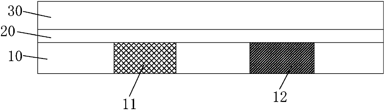
[0064] On the surface of the substrate, an interconnect dielectric layer 10 is formed by using a damascene process, such as figure 1 As shown, the above-mentioned interconnection medium layer 10 includes a plurality of first interconnection parts 11 and second interconnection parts 12 arranged alternately at intervals;

[0065] Depositing silicon nitride on the surface of the interconnect dielectric layer 10 to form a first etch barrier layer 20 with a thickness of 500nm;

[0066] SiO is formed on the first etch stop layer 20 2 layer, forming figure 1 The first dielectric layer 30 shown;

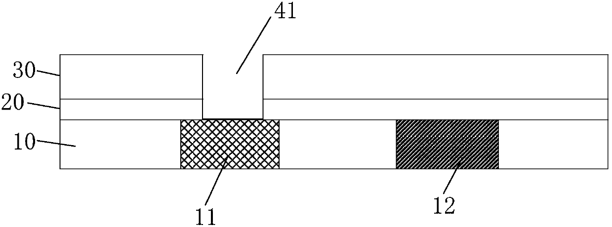
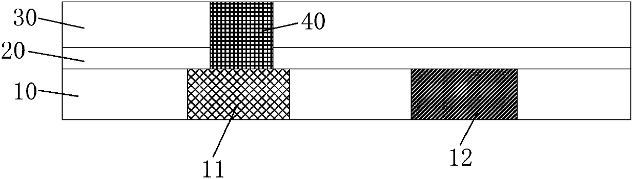
[0067] A first through hole 41 is opened in the above-mentioned first etch stop layer 20 and the above-mentioned first dielectric layer 30 above the above-mentioned first interconnection part 11, as figure 2 shown, and fil...

Embodiment 2

[0077] The difference from Embodiment 1 lies in that the thickness of the second etching barrier layer 90 is 650 nm, and the calculated selectivity ratio of the etching solution is 8.


PUM

PropertyMeasurementUnit
Thicknessaaaaaaaaaa
Thicknessaaaaaaaaaa
Thicknessaaaaaaaaaa

Abstract

The invention provides an MRAM device and a manufacturing method thereof. The manufacturing method comprises the steps of S1, arranging a first interconnection part and a second interconnection part in an interconnection dielectric layer; S2, sequentially arranging a first etching barrier layer and a first dielectric layer on a surface of the interconnection dielectric layer; S3, forming first metal holes in the first etching barrier layer and the first dielectric layer above a first interconnection part; S4, sequentially arranging a bottom electrode, an MTJ unit, a top electrode and a secondetching barrier layer on a surface of the first dielectric layer above the first interconnection part; S5, sequentially arranging a third dielectric layer, a third etching barrier layer and a fourth dielectric layer on a surface, far away from the first dielectric layer, of the second dielectric layer; S6, forming a second through hole and a third through hole; and S7, filling the second through hole and the third through hole with metal. The manufacturing method is advantaged in that process difficulty is reduced, and the cost rate of the device is improved.

Description

technical field [0001] The present application relates to the field of memory, and in particular, relates to an MRAM device and a manufacturing method thereof. Background technique [0002] In the prior art, an MRAM device includes a logic area and a storage area, the logic area is mainly a switching device, the storage area is mainly an MTJ device, and the MTJ device includes a bottom electrode, an MTJ unit and a top electrode. [0003] At present, the height difference between the interconnection structure above the top electrode and the interconnection structure above the logic area is relatively large. At the same time, another via hole needs to be opened in the dielectric layer of the storage area. The height difference between the two via holes is large, and the requirements for the etching selection ratio are very high. The process is difficult and the yield rate of the finished product is low. . Contents of the invention [0004] The main purpose of the present a...

Claims


Application Information

Patent Timeline
IPC IPC(8): H01L21/768H01L23/538H01L27/22
CPCH01L23/5386H01L21/76897H01L21/76832H10B61/00
Inventor 郑富强左正笏
Owner CETHIK GRP
Why Eureka
Try Eureka