A method for slicing heterojunction shingled solar cells

A solar cell and heterojunction technology, applied in circuits, photovoltaic power generation, electrical components, etc., can solve the problems affecting the efficiency and stability of shingled components, affecting the performance of solar cells, and destroying the amorphous silicon layer, and achieving the benefits of large Large-scale automated production, improved performance and reliability, and the effect of avoiding increased leakage current

Active Publication Date: 2022-02-08
福建钜能电力有限公司
View PDF5 Cites 0 Cited by
  • Summary
  • Abstract
  • Description
  • Claims
  • Application Information

AI Technical Summary

Problems solved by technology

[0003] The processing temperature of all processes of heterojunction solar cells is lower than 250°C. If the temperature is too high, the amorphous silicon layer of heterojunction solar cells will be destroyed, which will affect the performance of solar cells.
After the heterojunction cell is cut by laser, the laser generates local high temperature, the amorphous silicon layer at the edge of the laser cutting is damaged, the leakage current of the small cell after cutting increases, and the fill factor decreases, which affects the efficiency and efficiency of the shingled module. stability

Method used


Image

  • A method for slicing heterojunction shingled solar cells
  • A method for slicing heterojunction shingled solar cells
  • A method for slicing heterojunction shingled solar cells

Examples


Embodiment

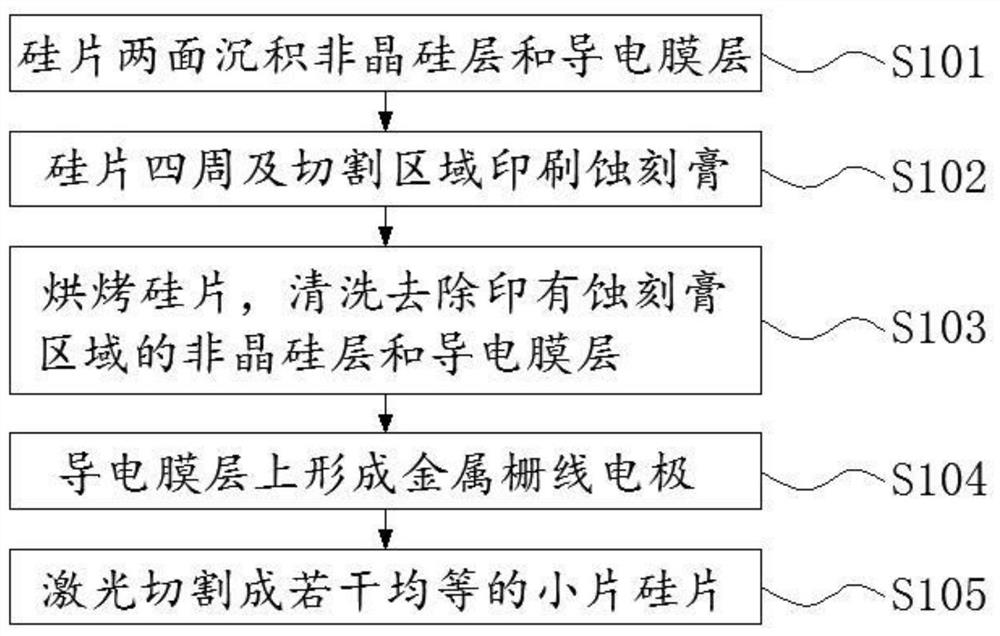
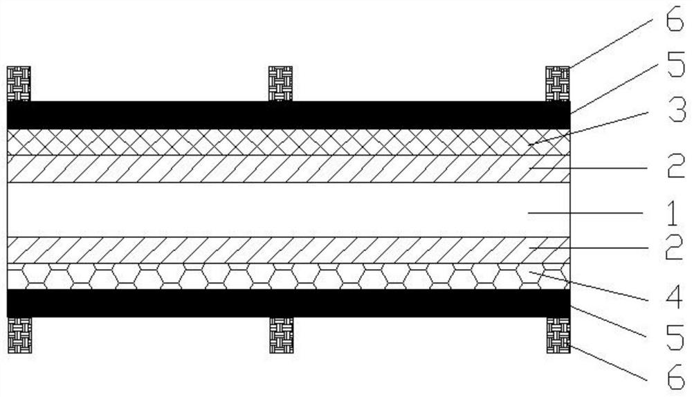
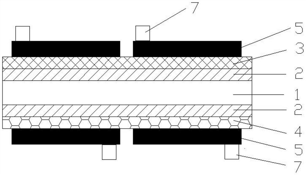
[0026] refer to Figure 1 ~ Figure 3 As shown, the present invention is a method for slicing heterojunction shingled solar cells, the method comprising the following steps:

[0027] Step S101, depositing a thin intrinsic amorphous silicon layer 2 and an n-type amorphous silicon layer 3 on one side of the n-type silicon wafer substrate 1 with a textured surface after cleaning, and depositing a thin intrinsic amorphous silicon layer 2 and a p-type amorphous silicon layer on the other side amorphous silicon layer 4, and deposit a conductive film layer 5 on the n-type amorphous silicon layer 3 and the p-type amorphous silicon layer 4, the conductive film layer is deposited by magnetron sputtering, and the conductive film layer is transparent and conductive An oxide film layer or a composite film layer of a transparent conductive oxide film layer and a metal film layer, the transparent conductive oxide film layer includes ITO, AZO, IGZO and doped indium oxide, and the metal film la...


PUM

PropertyMeasurementUnit
widthaaaaaaaaaa
viscosityaaaaaaaaaa
wavelengthaaaaaaaaaa

Abstract

The invention discloses a method for slicing heterojunction shingled solar cells, which comprises the following steps: depositing a thin intrinsic amorphous silicon layer and an n-type amorphous silicon layer on one side of an n-type silicon wafer, and depositing a thin intrinsic amorphous silicon layer on the other side. sign amorphous silicon layer and p-type amorphous silicon layer, and deposit conductive film layer on n-type amorphous silicon layer and p-type amorphous silicon layer; Print etching paste on the conductive film layer; bake the n-type silicon wafer printed with etching paste, clean and remove the amorphous silicon layer and conductive film layer in the area printed with etching paste on the n-type silicon wafer; conduct electricity on the n-type silicon wafer A metal grid line electrode is formed on the film layer; several equal small pieces of n-type silicon wafers are cut by laser in the n-type silicon wafer cutting area. The invention uses printing to print etching paste on the double-sided edge and cutting area of ​​the n-type silicon wafer, removes the amorphous silicon layer and the conductive film layer, improves the performance and reliability of the heterojunction shingled solar cell, and has a simple process , conducive to large-scale automated production.

Description

technical field [0001] The invention relates to the technical field of solar cell manufacturing, in particular to a slicing method for heterojunction shingled solar cells. Background technique [0002] Shingled solar module is a kind of small battery that cuts traditional solar cells into more than 2 pieces. The front main grid and the back electrode of two adjacent battery cells overlap, and then they are connected in series with a special material similar to conductive glue. Form a long battery string together, and connect multiple battery strings in series and parallel to form a high-density solar module technology. This kind of solar shingled module improves the uniformity of current density and reduces the current transmission impedance, thereby reducing the internal power consumption of the module. At the same time, the innovative string arrangement reduces the conventional inter-sheet spacing and increases the light-receiving area, so it can Improve the power generat...

Claims


Application Information

Patent Timeline
Patent Type & Authority Patents(China)
IPC IPC(8): H01L21/304H01L31/18
CPCH01L31/1876H01L21/3043Y02E10/50Y02P70/50
Inventor 黄辉明庄辉虎罗骞张杰宋广华
Owner 福建钜能电力有限公司
Why Eureka
Try Eureka