Liquid crystal display panel and manufacturing method thereof

A technology for a liquid crystal display panel and a manufacturing method, applied in optics, instruments, nonlinear optics, etc., can solve problems such as difficulty in meeting expected requirements and low yield, and achieve the effects of reducing cell thickness, speeding up response time, and simple process

Inactive Publication Date: 2020-01-14
NANJING CEC PANDA LCD TECH
View PDF4 Cites 0 Cited by
  • Summary
  • Abstract
  • Description
  • Claims
  • Application Information

AI Technical Summary

Problems solved by technology

[0004] At present, the low box thickness is mainly achieved by reducing the column height of the spacer, but due to process limitations, the change of the column height is limited. The lower the box thickness, the higher the requirements for the formation process of the spacer and the lower the yield rate. Therefore, simply reducing the column height of the spacer is difficult to meet the expected requirements.

Method used


Image

  • Liquid crystal display panel and manufacturing method thereof
  • Liquid crystal display panel and manufacturing method thereof

Examples


Embodiment 1

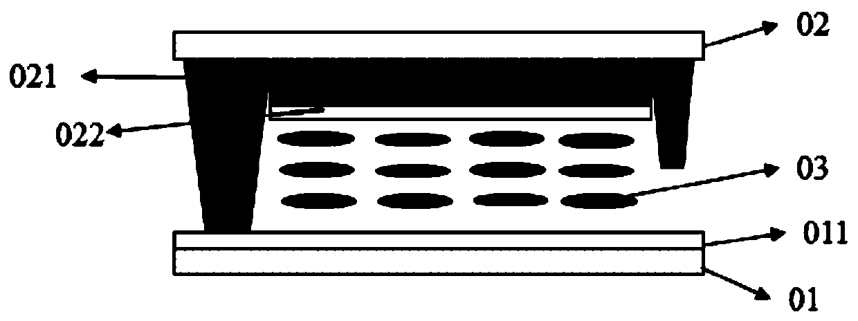
[0037] This embodiment discloses a method for manufacturing a liquid crystal display panel. The manufactured liquid crystal display panel is as follows: figure 1 Shown, for FFS / IPS display mode. The liquid crystal display panel includes an array substrate 01, a color filter substrate 02, and a liquid crystal 03 located between the array substrate 01 and the color filter substrate 02, wherein the array substrate 01 is an array substrate conforming to a conventional FFS / IPS display mode, and the color filter The substrate 02 is a color filter substrate conforming to the conventional FFS / IPS display mode, and the liquid crystal 03 is a positive liquid crystal or a negative liquid crystal, wherein, because the liquid crystal display panel is suitable for the FFS / IPS display mode, the liquid crystal 03 in the display panel Arranged horizontally. The preparation method comprises the following steps:

[0038] S1: Coating an alignment liquid on the side of the array substrate 01 opp...

Embodiment 2

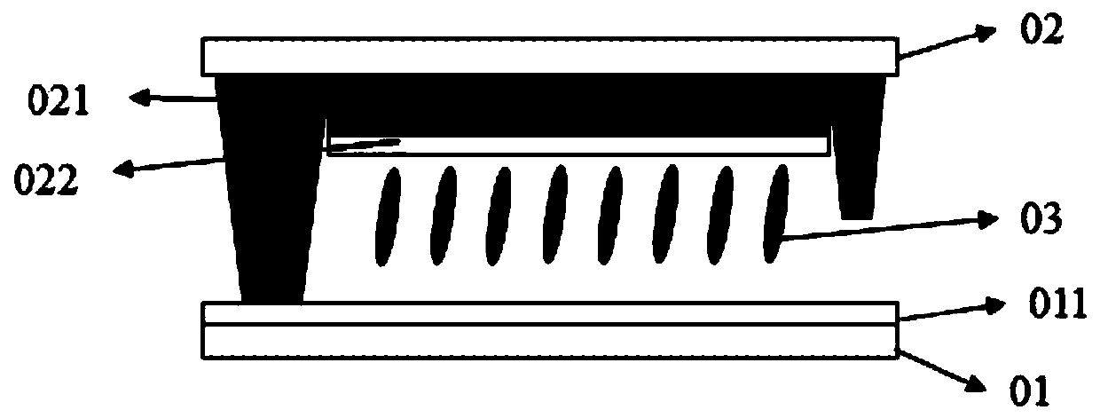
[0043]This embodiment discloses a method for manufacturing a liquid crystal display panel. The manufactured liquid crystal display panel is as follows: figure 2 shown, for VA display mode. The liquid crystal display panel includes an array substrate 01, a color filter substrate 02, and a liquid crystal 03 located between the array substrate 01 and the color filter substrate 02, wherein the array substrate 01 is an array substrate conforming to a conventional VA display mode, and the color filter substrate 02 In order to comply with the color filter substrate of the conventional VA display mode, the liquid crystal 03 is a negative liquid crystal, wherein, because the liquid crystal display panel is suitable for the VA display mode, the liquid crystal 03 in the display panel is arranged vertically. The preparation method comprises the following steps:

[0044] S1: Coating an alignment liquid on the side of the array substrate 01 opposite to the color filter substrate 02 to for...


PUM

PropertyMeasurementUnit
wavelengthaaaaaaaaaa

Abstract

The invention provides a liquid crystal display panel and a manufacturing method thereof, and relates to the field of liquid crystal display panels. The manufacturing method of the liquid crystal display panel comprises the steps of S1, coating the side, which is opposite to a color film substrate, of an array substrate with alignment liquid to form a first alignment film layer; S2, preprocessingthe side, which is opposite to the array substrate, of the color film substrate by adopting a polymer monomer; S3, injecting the liquid crystal added with a polymerizable monomer and an alignable monomer into the array substrate or the color film substrate, and then aligning and laminating the array substrate and the color film substrate to form a panel; and S4, firstly, irradiating the laminatedpanel from the side of the array substrate by adopting ultraviolet light with a first wavelength to enable the polymer monomer of the liquid crystal to form a polymer film layer on one side of the color film substrate, and irradiating the laminated panel from the side of the array substrate by adopting ultraviolet light with a second wavelength to enable the alignment liquid monomer of the liquidcrystal to form a second alignment film layer on the polymer film layer, wherein the first wavelength is greater than the second wavelength.

Description

technical field [0001] The invention belongs to the field of liquid crystal display panels, and in particular relates to a liquid crystal display panel and a manufacturing method thereof. [0002] technical background [0003] Liquid Crystal Display (LCD) has many advantages such as thin body, light weight, low power consumption, and high resolution, and is widely used in products such as TVs, smart phones, notebook computers, and flat panel displays. With the improvement of living standards and the vigorous development of the e-sports industry, consumers' demand for full-color and high-definition sports videos has become more and more intense, and response time has gradually become a major factor restricting the development of liquid crystal displays. At present, although the rise time of the nematic liquid crystal used in the liquid crystal panel can be improved by increasing the voltage, it is difficult to change the fall time due to the characteristics of the nematic liqu...

Claims


Application Information

Patent Timeline
Patent Type & Authority Applications(China)
IPC IPC(8): G02F1/1337G02F1/1339G02F1/1333
CPCG02F1/1333G02F1/133711G02F1/133784G02F1/1339
Inventor 张卫锴
Owner NANJING CEC PANDA LCD TECH
Why Eureka
Try Eureka