Double-T-shaped nano gate and preparation method thereof

A nanometer and gate cap technology, used in semiconductor/solid-state device manufacturing, electrical components, circuits, etc., can solve the problem of high parasitic capacitance of dielectric-assisted T-type nanometer gates, reduce gate parasitic capacitance, avoid inverted gates, reduce Effects of Parasitic Capacitance

Active Publication Date: 2020-01-17
THE 13TH RES INST OF CHINA ELECTRONICS TECH GRP CORP
View PDF19 Cites 4 Cited by
  • Summary
  • Abstract
  • Description
  • Claims
  • Application Information

AI Technical Summary

Problems solved by technology

[0004] Aiming at the problem of high parasitic capacitance of the dielectric-assisted T-type nano-gate prepa...

Method used


Image

  • Double-T-shaped nano gate and preparation method thereof
  • Double-T-shaped nano gate and preparation method thereof
  • Double-T-shaped nano gate and preparation method thereof

Examples


Embodiment Construction

[0049]In order to make the object, technical solution and advantages of the present invention more clear, the present invention will be further described in detail below in conjunction with the examples. It should be understood that the specific embodiments described here are only used to explain the present invention, not to limit the present invention.

[0050] The present invention will be further described in detail below in conjunction with the accompanying drawings and specific embodiments.

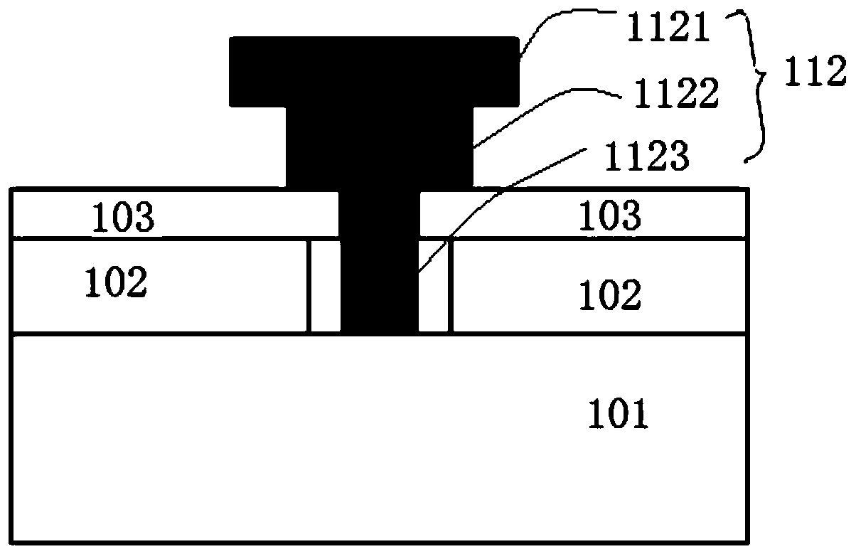
[0051] For an example, see figure 1 , the embodiment of the present invention provides a double T-shaped nano-gate 112, including a grid cap 1121, a grid waist 1122 and a grid root 1123, the width of the grid cap 1121 is greater than the width of the grid waist 1122, and the width of the grid waist 1122 is greater than The width of the grid root 1123 . The double T-shaped nano-gate 112 is grown on the substrate 101, and the bottom dielectric passivation layer 102 and the top diele...


PUM

PropertyMeasurementUnit
Thicknessaaaaaaaaaa
Thicknessaaaaaaaaaa
Thicknessaaaaaaaaaa

Abstract

The invention relates to the technical field of microelectronic devices, and particularly discloses a double-T-shaped nano gate and a preparation method thereof. The double-T-shaped nano gate grows ona substrate with a dielectric passivation layer, and the dielectric passivation layer comprises a bottom dielectric passivation layer and a top dielectric passivation layer; the double-T-shaped nanogate sequentially comprises a gate root, a gate waist and a gate cap from bottom to top. The gate root penetrates through the dielectric passivation layer and grows on the substrate, the gate root isnot in contact with the bottom dielectric passivation layer, and the lower surface of the gate waist is in contact with the upper surface of the top dielectric passivation layer. The grid root and thegrid cap of the double-T-shaped nano grid provided by the invention are suspended; the contact with the dielectric passivation layer is avoided; the top dielectric passivation layer is covered with the gate waist, the stability of the double-T-shaped gate is improved, the distance between the gate cap and the dielectric passivation layer is increased through the double-T-shaped structure, parasitic capacitance can be further reduced, gate inversion caused by the fact that no dielectric support exists during gate stripping is avoided, and the purpose of improving the frequency characteristic of the device is achieved.

Description

technical field [0001] The invention relates to the technical field of microelectronic devices, in particular to a double T-shaped nano-gate and a preparation method thereof. Background technique [0002] The performance of the high electron mobility transistor (HEMT) device is closely related to the processing technology of the device, especially the fabrication of the gate line plays a decisive role in the device. The smaller the gate length, the current cut-off frequency of the device (f T ) The higher the noise figure of the device is, the smaller the noise figure of the device is. People can obtain devices with better characteristics by continuously reducing the gate length of HEMT devices. At present, the gate length of advanced GaAs, InP, and GaN devices at home and abroad has been reduced to less than 100nm. However, as the gate length shortens, the gate resistance increases, and the increase in gate resistance becomes one of the important factors restricting the pe...

Claims


Application Information

Patent Timeline
IPC IPC(8): H01L29/423H01L21/285
CPCH01L29/42316H01L21/28537H01L21/28581H01L21/28587Y02P70/50
Inventor 顾国栋吕元杰敦少博梁士雄冯志红
Owner THE 13TH RES INST OF CHINA ELECTRONICS TECH GRP CORP
Why Eureka
Try Eureka