Forming conductive vias using a light guide

A technology of light guide and photoresist, which is applied in the formation of electrical connections of printed components, originals for photomechanical processing, optics, etc., which can solve problems such as expensive processes, limiting high-speed PCB density and complexity, etc.

Active Publication Date: 2020-01-17
IBM CORP
View PDF17 Cites 1 Cited by
  • Summary
  • Abstract
  • Description
  • Claims
  • Application Information

AI Technical Summary

Problems solved by technology

Existing processes are extremely expensive, a significant source of manufacturi...

Method used


Image

  • Forming conductive vias using a light guide
  • Forming conductive vias using a light guide
  • Forming conductive vias using a light guide

Examples


Embodiment Construction

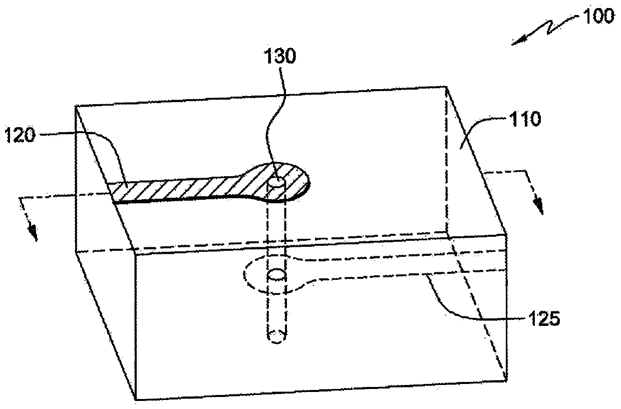
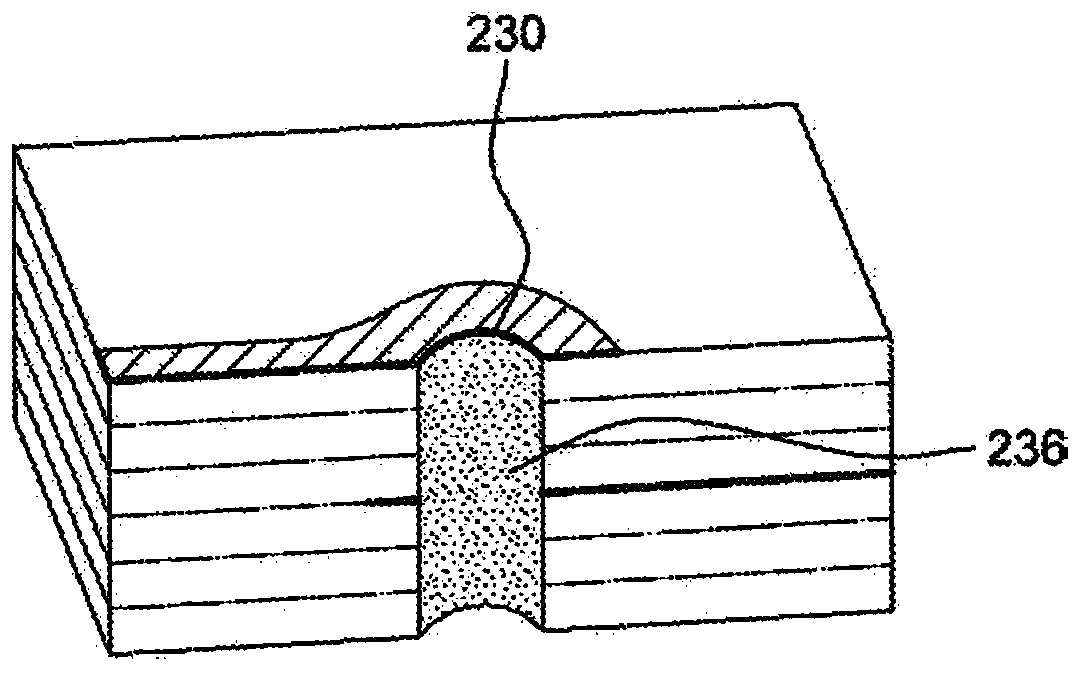
[0036] The present invention provides a method and structure. In an exemplary embodiment, the method includes: providing a through hole in a base material in a direction perpendicular to a plane of the base material; applying a photoresist layer to an inner surface of the through hole, inserting a light guide into the through hole In the through hole, a portion of the photoresist layer is exposed through the light guide, thereby generating an exposed portion of the photoresist layer and an unexposed portion of the photoresist layer, removing the a portion of the photoresist layer and metal plated the area of ​​the through hole from which the photoresist layer was removed, thereby obtaining the metal plated portion of the through hole and the through hole. The portion of the hole that is not plated with metal.

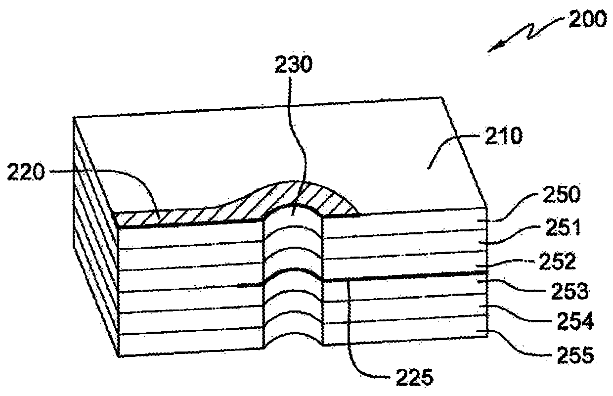
[0037] In an exemplary embodiment, the method includes providing a via in a base material including at least two copper lines and at least one insulating layer separat...


PUM


Abstract

The present invention provides a process and a structure of forming conductive vias using a light guide. In an exemplary embodiment, the process includes providing a via in a base material in a direction perpendicular to a plane of the base material, applying a photoresist layer to an interior surface of the via, inserting a light guide into the via, exposing, by the light guide, a portion of thephotoresist layer to light, thereby resulting in an exposed portion of the photoresist layer and an unexposed portion of the photoresist layer, removing a portion of the photoresist layer, and platingan area of the via, where the photoresist has been removed, with a metal, thereby resulting in a portion of the via plated with metal and a portion of the via not plated with metal.

Description

technical field [0001] The present disclosure relates to conductive vias in printed circuit boards (PCBs), and more particularly, to the use of light guides to form conductive vias. Background technique [0002] Existing techniques for PCB via stub removal require either (a) machining (drilling, milling, etc.) or (b) a laser "drilling" process to remove the unwanted conductive portion of the via barrel. While both of these existing processes are successful in reducing through-hole stub lengths, they are prohibitively expensive, a significant source of manufacturing defects, rarely 100 percent successful, and most importantly, limit the density and complexity of high-speed PCBs . [0003] Numerous techniques exist for back-drilling and laser removal of PCB vias. Existing processes are extremely expensive, a significant source of manufacturing defects and, most importantly, limit the density and complexity of high-speed PCBs. Known methods include (a) machining methods to r...

Claims


Application Information

Patent Timeline
IPC IPC(8): H05K3/42
CPCH05K3/428H05K3/429H05K2201/09645H05K2203/0514H05K2203/1383H05K3/424G03F1/38G03F7/038G03F7/039G03F7/16G03F7/20G03F7/26G03F7/405H05K3/4038H05K2203/0562
Inventor G·巴特利M·多伊尔D·贝克尔M·珍森
Owner IBM CORP
Why Eureka
Try Eureka