Pole-zero tracking compensation network for voltage regulators
A technology of compensation network and regulator, applied in the field of compensation network
- Summary
- Abstract
- Description
- Claims
- Application Information
AI Technical Summary
Problems solved by technology
Method used
Image

Examples
Embodiment Construction
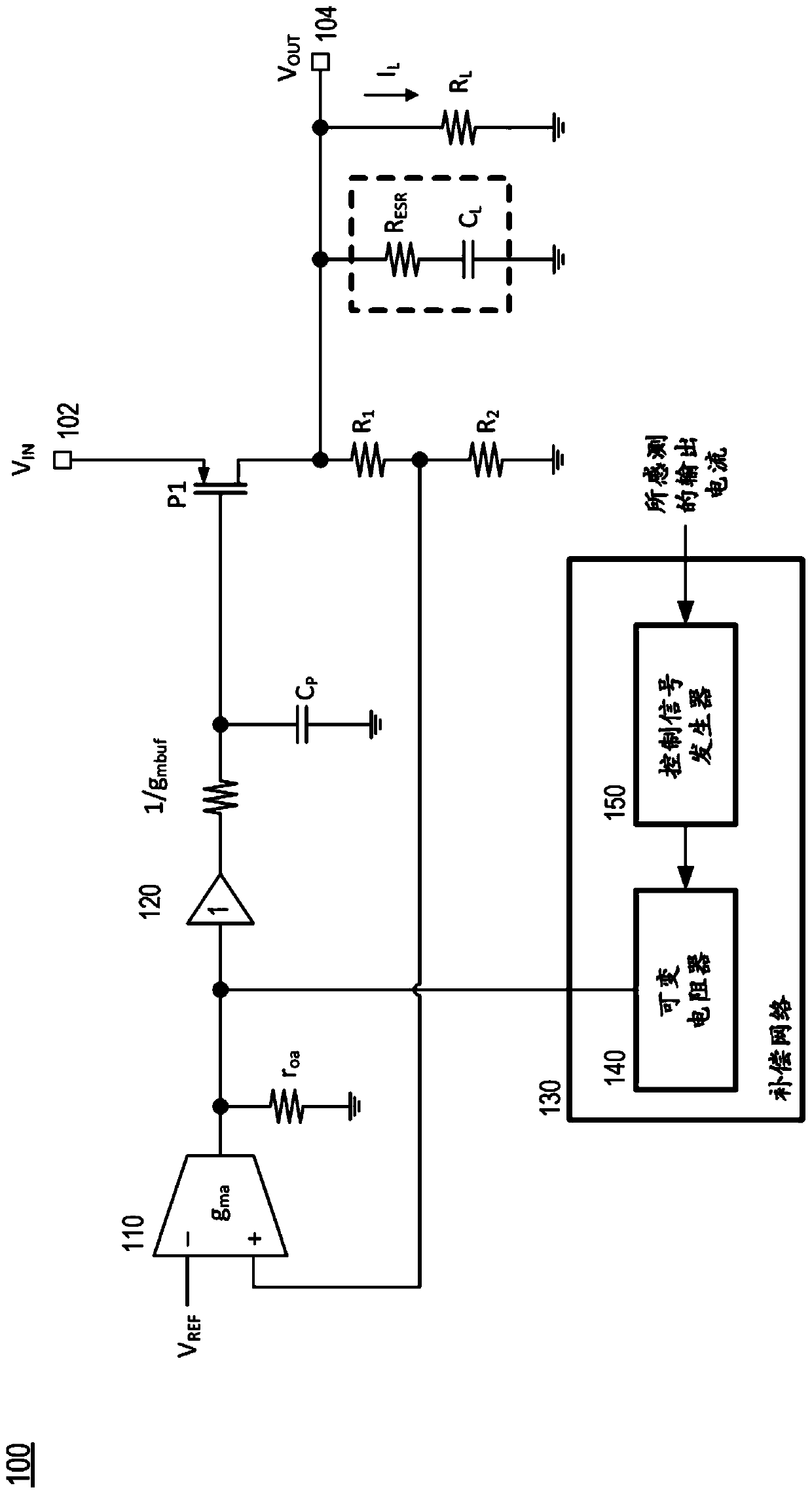
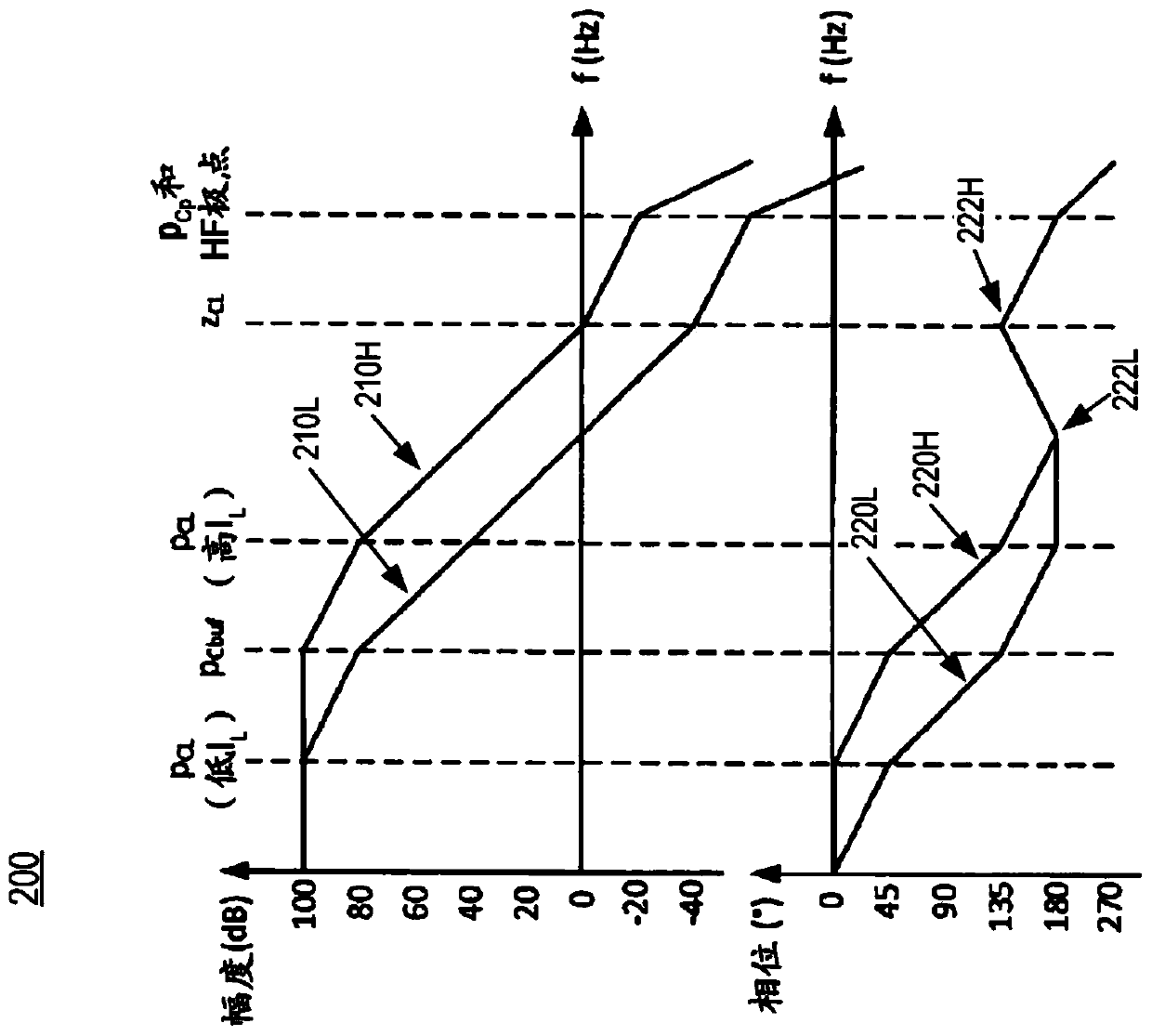
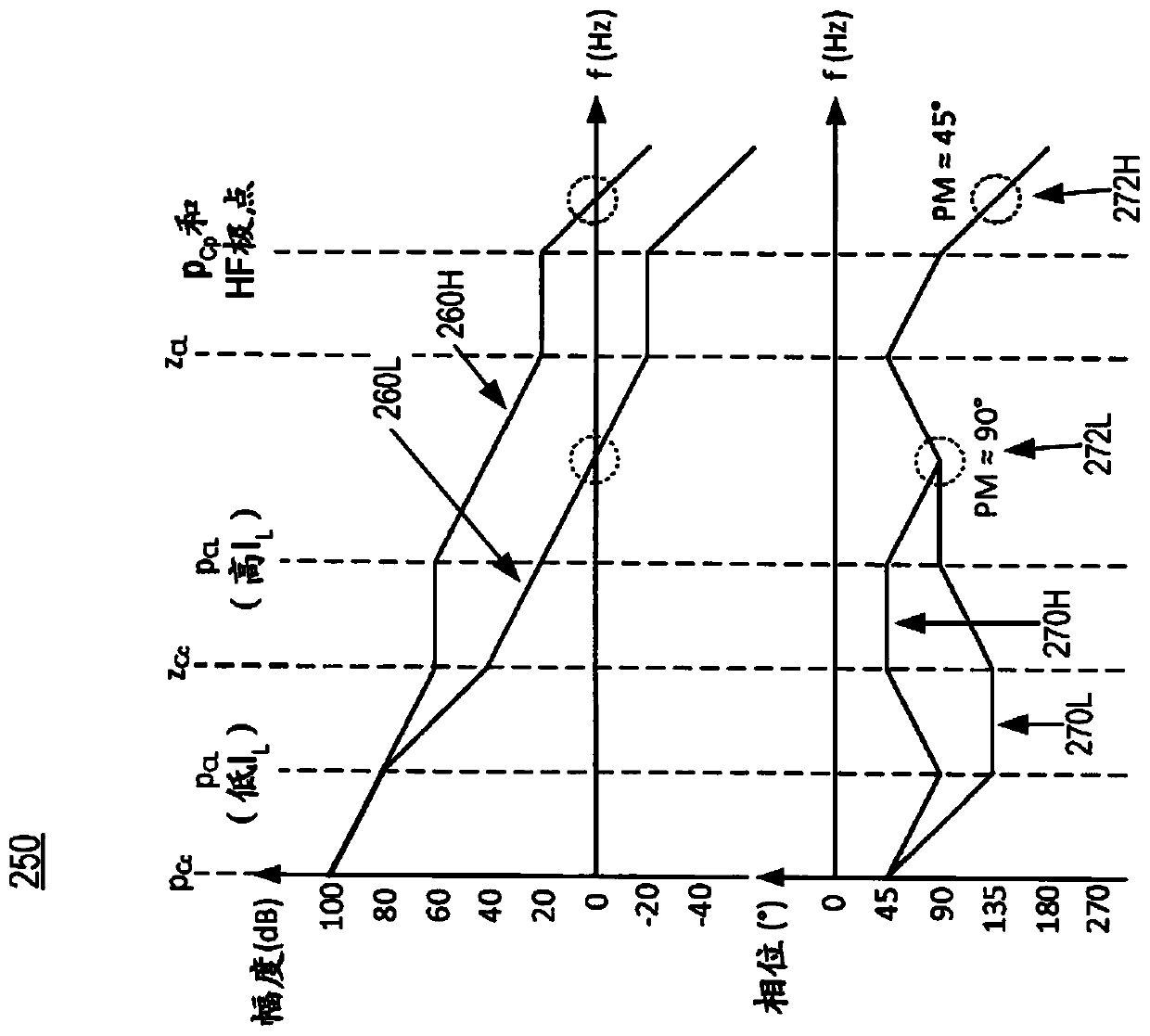
[0020] Embodiments described herein provide compensation networks and associated methods for compensating the frequency and phase response of a linear regulator to ensure stable operation of the regulator over a wide range of output currents. Embodiments are primarily described in the context of a low dropout (LDO) linear regulator using a p-channel metal oxide semiconductor field effect transistor (pMOSFET) as the pass device. However, the invention is not limited to LDO regulators based on such transfer devices. For example, the compensation network described can be readily used with LDO regulators using PNP bipolar junction transistors (BJTs) that have similar impedance characteristics (and associated poles) to pMOSFET pass devices. Still further, linear regulators using other types of pass devices (eg, NPN BJT, n-channel MOSFET) may also advantageously use the compensation network described below. Still further, the described compensation network can be used to stabilize ...
PUM
 Abstract
Description
Claims
Application Information