Electroless nickel immersion gold surface treatment method for polyphenyl ether-containing printed circuit board

A printed circuit board, chemical nickel gold technology, applied in the field of chemical nickel gold surface treatment of polyphenylene ether-containing printed circuit boards, can solve the problems of chemical nickel gold whitening and degolding, reduce precipitates, and reduce gold staining effect of influence

Active Publication Date: 2020-01-21
WUS PRINTED CIRCUIT (KUNSHAN) CO LTD
View PDF6 Cites 1 Cited by
  • Summary
  • Abstract
  • Description
  • Claims
  • Application Information

AI Technical Summary

Problems solved by technology

[0003] The purpose of the present invention is to provide a method for surface treatment of polyphenylene ether-containing printed circuit boards with chemical nickel and gold, so as to solve the problem of chemical nickel-gold whitening of polyphenylene ether-containing printed circuit boards in the prior art after chemical nickel-gold treatment Technical problems of degolding

Method used


Image

  • Electroless nickel immersion gold surface treatment method for polyphenyl ether-containing printed circuit board
  • Electroless nickel immersion gold surface treatment method for polyphenyl ether-containing printed circuit board
  • Electroless nickel immersion gold surface treatment method for polyphenyl ether-containing printed circuit board

Examples


Embodiment Construction

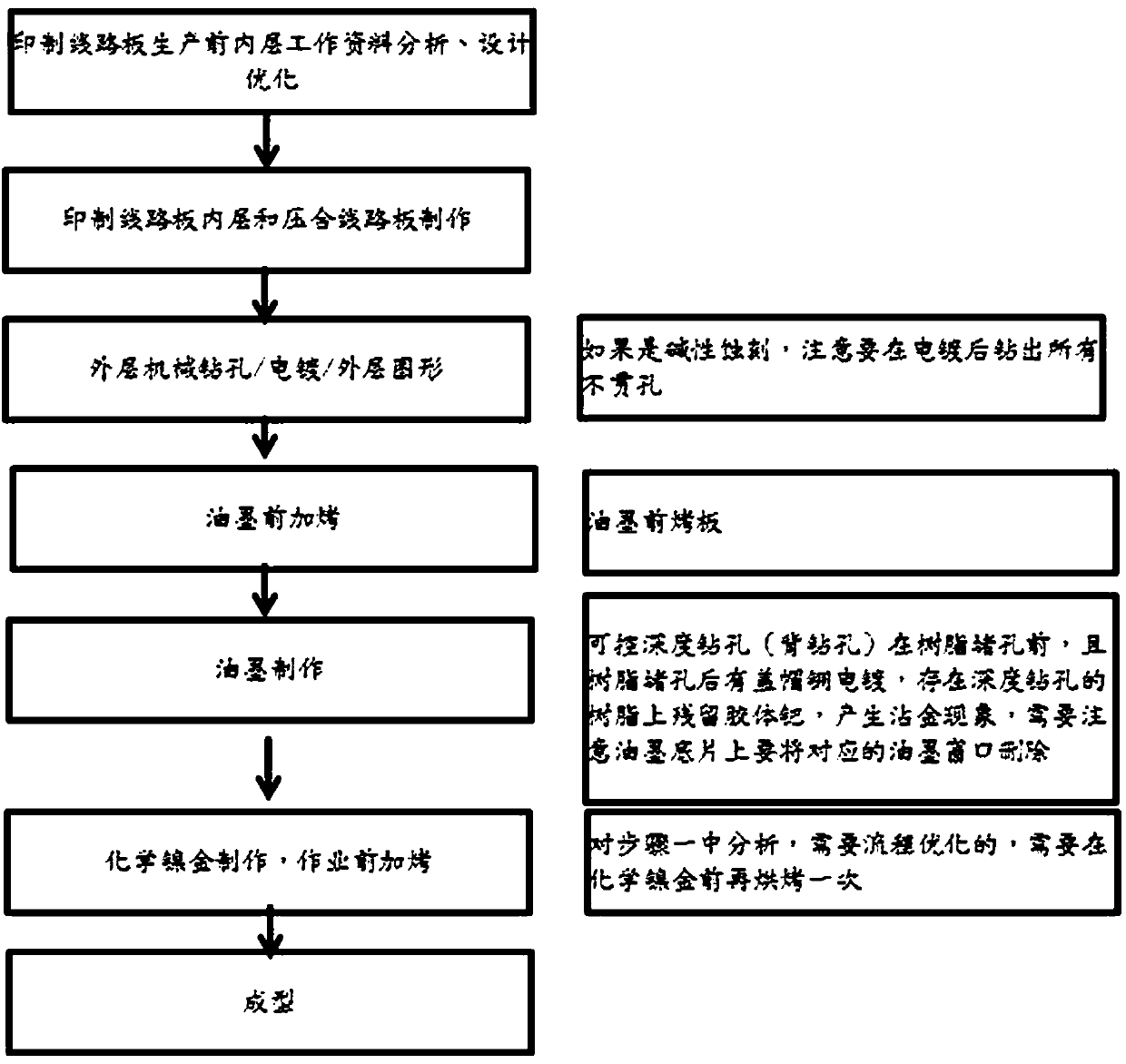
[0032] The present invention will be further described below in conjunction with the accompanying drawings. The following examples are only used to illustrate the technical solution of the present invention more clearly, but not to limit the protection scope of the present invention.

[0033] Such as figure 1 Shown, a kind of method that contains polyphenylene ether printed circuit board chemical nickel-gold surface treatment, comprises

[0034] a. Data analysis and optimization design of the inner layer of the circuit board;

[0035] b. Print the inner layer of the printed circuit board and press the circuit board;

[0036] c. Mechanical drilling of the outer layer of the circuit board, copper electroplating and outer graphic production;

[0037] d. Execute the baking process;

[0038] e. Ink production;

[0039] f. Execute the baking process;

[0040] g. Carry out chemical nickel-gold treatment.

[0041] Inner layer data analysis and design optimization before printed...


PUM


Abstract

The invention discloses an electroless nickel immersion gold surface treatment method for a polyphenyl ether-containing printed circuit board in the technical field of surface treatment of printed circuit boards, and aims to solve the technical problem of electroless nickel immersion gold whitening and gold removing of a polyphenyl ether-containing printed circuit board after electroless nickel immersion gold treatment in the prior art. The method comprises the following steps: carrying out circuit board inner layer data analysis and optimal design; printing an inner layer of a circuit board and laminating the circuit board; mechanically drilling an outer layer of the circuit board, electroplating copper and manufacturing an outer layer pattern; executing a baking process; preparing printing ink; executing a baking process; and carrying out electroless nickel immersion gold. According to the invention, a shielding copper foil and a dummy pad are additionally arranged on a secondary outer layer, and a baking process is added to the board after etching. Because the board is baked after etching, it is guaranteed that material precipitates are reduced, and it is also guaranteed that the influence on nickel deposition is the minimum during electroless nickel immersion gold. Moreover, by carrying out secondary drilling and covering holes with ink, the influence of the baking processon gold staining of non-through holes and gold staining in a deep drilling resin hole-plugging process is reduced.

Description

technical field [0001] The invention belongs to the technical field of surface treatment of printed circuit boards, and in particular relates to a method for chemical nickel-gold surface treatment of printed circuit boards containing polyphenylene ether. Background technique [0002] With the increase in the use of high-speed materials for printed circuit boards (Printer circuit board / PCB), the use of high-speed materials containing PPO (polyphenylene ether) is also increasing. Due to the consideration of assembly factors, the surface treatment of printed circuit boards It is chemical nickel gold, and when it is designed in this way, the residual small molecule solvent in the material will volatilize and precipitate out during the production process, and when the nickel bath reacts, these small molecule substances will affect the deposition of nickel, on the substrate and copper pad Thin plating is produced at the handover position, and the nickel deposition at this position...

Claims


Application Information

Patent Timeline
Patent Type & Authority Applications(China)
IPC IPC(8): H05K3/00H05K3/24H05K1/02
CPCH05K1/0296H05K3/00H05K3/24H05K2203/1105H05K2203/30
Inventor 刘培辉曹智宏杨益
Owner WUS PRINTED CIRCUIT (KUNSHAN) CO LTD
Why Eureka
Try Eureka