Method for coating phosphor powder layer on LED chip and manufacture of LED device

An LED chip and phosphor layer technology, applied in semiconductor devices, electrical components, circuits, etc., can solve the problems of difficult to control consistency, high cost, and poor consistency of the amount of phosphor powder in LED chips, so as to achieve a small effect of phosphor deposition. , The effect of short curing time and simple process

Active Publication Date: 2011-09-28
FOSHAN NATIONSTAR OPTOELECTRONICS CO LTD
View PDF2 Cites 0 Cited by
  • Summary
  • Abstract
  • Description
  • Claims
  • Application Information

AI Technical Summary

Problems solved by technology

However, due to factors such as the instability of the air pressure and the precipitation of the phosphor powder in the actual production process, the consistency of the phosphor powder distributed on each LED chip is relatively poor.
With the development of science and technology, some new coating processes have also appeared in recent years: 1) as the publication number of CN1897312 in the Chinese Invention Patent Application Publication, a vacuum sputtering coating phosphor process is disclosed, although it has the advantage of uniform coating , but due to the influence of the physical characteristics of phosphor particles, the possibility of this process is very small, and the cost is relatively high; 2) For example, the patent document of US Patent Publication No. 20030181122 discloses a patterned coating for photolithography development Phosphor powder technology, although the phosphor coating structure can be adjusted according to the characteristics of the chip, but due to the influence of the characteristics of the photoresist material, the luminous efficiency of the product decays quickly; The impact of powder precipitation also has the problem of difficult control of consistency, which is not suitable for mass production

Method used


Image

  • Method for coating phosphor powder layer on LED chip and manufacture of LED device
  • Method for coating phosphor powder layer on LED chip and manufacture of LED device
  • Method for coating phosphor powder layer on LED chip and manufacture of LED device

Examples


Embodiment Construction

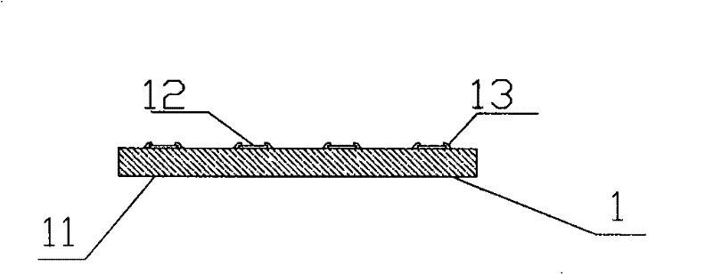
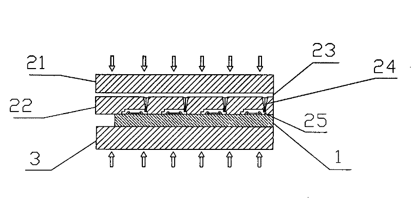
[0024] figure 1 Shown is a flowchart of a method for coating a phosphor layer on an LED chip in an embodiment of the present invention. see also Figure 2A ~ Figure 2D , utilize a mold to implement for the present invention figure 1 schematic diagram. In step S101 , the substrate 1 is prepared, and the phosphor powder mixture 4 is prepared, wherein the substrate 1 is mounted with LED chips 12 . In this embodiment, preparing the substrate 1 includes: dispensing glue, that is, dispensing an adhesive (not shown in the figure) on the substrate 1; bonding the LED chip 12 on the adhesive; connecting the leads 13, namely Connect the electrodes (not shown in the figure) on the LED chip 12 and the conductive layer (not shown in the figure) on the substrate to form a loop to obtain the following Figure 2A A substrate 1 on which LED chips 12 are mounted is shown. In this embodiment, the number of LED chips can be one, or two or more.

[0025] The preparation of the phosphor powder...


PUM


Abstract

The invention provides a method for coating a phosphor powder layer on an LED chip, which comprises the following steps: preparing a substrate, and preparing phosphor powder mixed glue, wherein the substrate is provided with the LED chip; preparing a die, arranging the substrate in the die, closing the die and applying pressure to form a cavity between the substrate and the die, wherein the die isprovided with a colloid passage and a die cavity corresponding to the position of the LED chip; injecting the phosphor powder mixed glue into the die cavity along the colloid passage, and making thephosphor powder mixed glue cover the LED chip and fill the cavity; solidifying and molding the phosphor powder mixed glue in the cavity; and after the injected phosphor powder mixed glue is solidified, separating the die from the substrate to make the phosphor powder mixed glue separated from the die and combined on the substrate so as to form the phosphor powder layer. The method for forming thephosphor powder layer by a die injection molding method has good consistency and simple process, and is suitable for mass production. In addition, the invention also provides a method for manufacturing an LED device based on the method for coating the phosphor powder layer on the LED chip.

Description

technical field [0001] The present invention relates to a method for coating phosphor powder and a method for manufacturing a semiconductor device, in particular to a method for coating a phosphor layer on a light emitting diode (Light Emitting Diode, LED) chip and the manufacture of an LED device based on the method method. Background technique [0002] A light emitting diode (Light Emitting Diode, LED) is a solid-state semiconductor device that can directly convert electricity into light. Because LEDs do not contain mercury, are small in size, long in life, fast in response, environmentally friendly, energy-saving, and have high color saturation, they are used more and more widely. The later third-generation lighting sources are widely used in liquid crystal projection devices, mobile phone backlights, and display screens. [0003] At present, there are many ways for LEDs to produce white light. One of them is that the blue chip excites the yellow phosphor powder to mix ...

Claims


Application Information

Patent Timeline
Patent Type & Authority Patents(China)
IPC IPC(8): H01L33/00
Inventor 余彬海李军政梁丽芳
Owner FOSHAN NATIONSTAR OPTOELECTRONICS CO LTD
Why Eureka
Try Eureka