Tin device for processing printed circuit boards

A printed circuit board and tin spot technology, which is applied in the direction of printed circuit, metal processing equipment, metal processing, etc., can solve the problems of circuit board skew, unfavorable soldering, and inability to maintain the level, so as to achieve the effect of preventing tilting and good soldering

Inactive Publication Date: 2020-01-24
陈强
View PDF8 Cites 4 Cited by
  • Summary
  • Abstract
  • Description
  • Claims
  • Application Information

AI Technical Summary

Problems solved by technology

[0003] Printed circuit boards are divided into single-sided boards, double-sided boards and multi-layer boards. When soldering, it is generally necessary to keep the circuit boards on a horizontal plane. Since both sides of the double-sided boards have structures, it is easy to make the circuit when placed on the workbench. The board is skewed and cannot be kept horizontal, and it tends to flow to the lower side during soldering, which is not conducive to soldering

Method used


Image

  • Tin device for processing printed circuit boards
  • Tin device for processing printed circuit boards
  • Tin device for processing printed circuit boards

Examples


Embodiment Construction

[0024] The following will clearly and completely describe the technical solutions in the embodiments of the present invention with reference to the accompanying drawings in the embodiments of the present invention. Obviously, the described embodiments are only some, not all, embodiments of the present invention. Based on the embodiments of the present invention, all other embodiments obtained by persons of ordinary skill in the art without making creative efforts belong to the protection scope of the present invention.

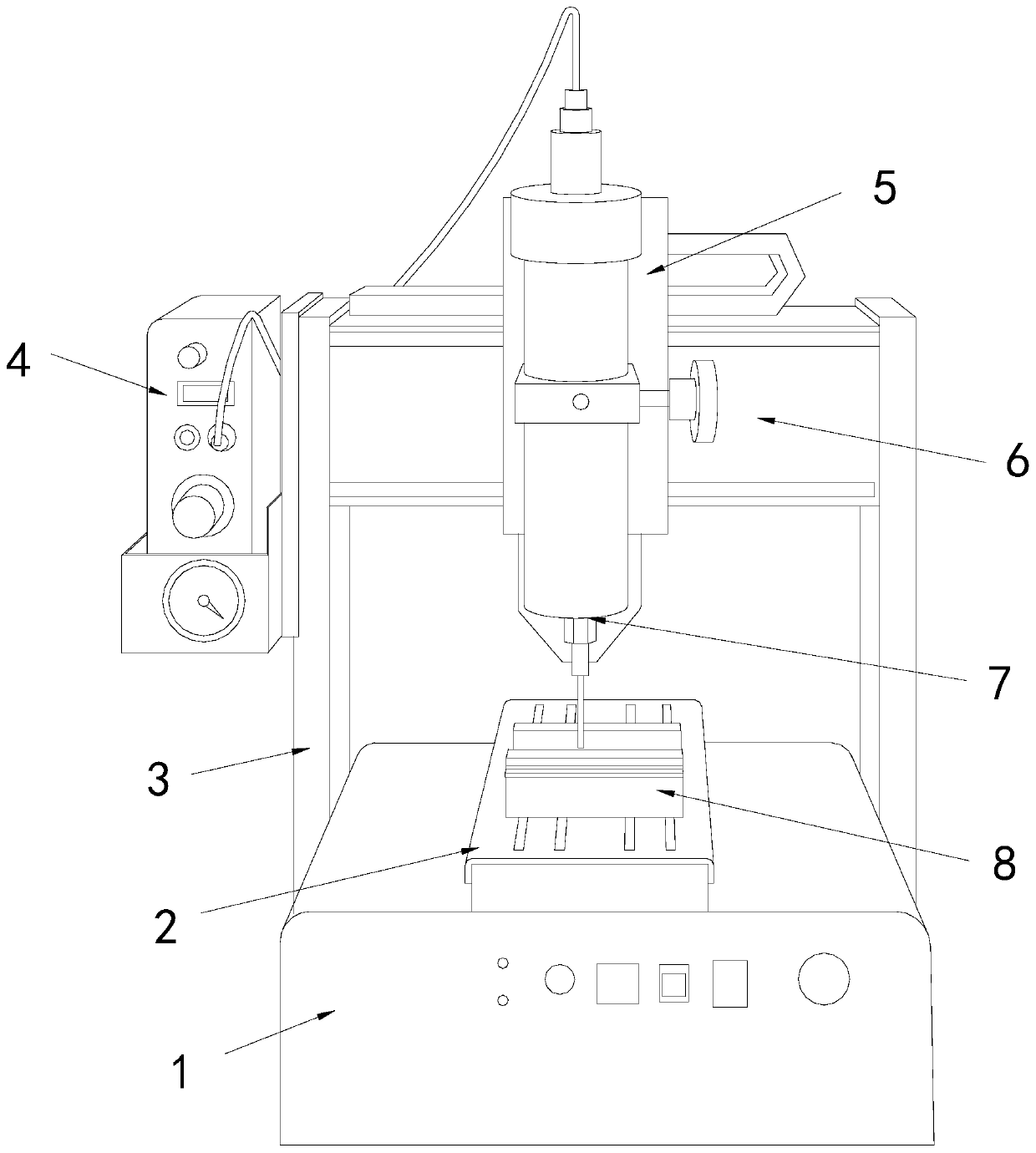
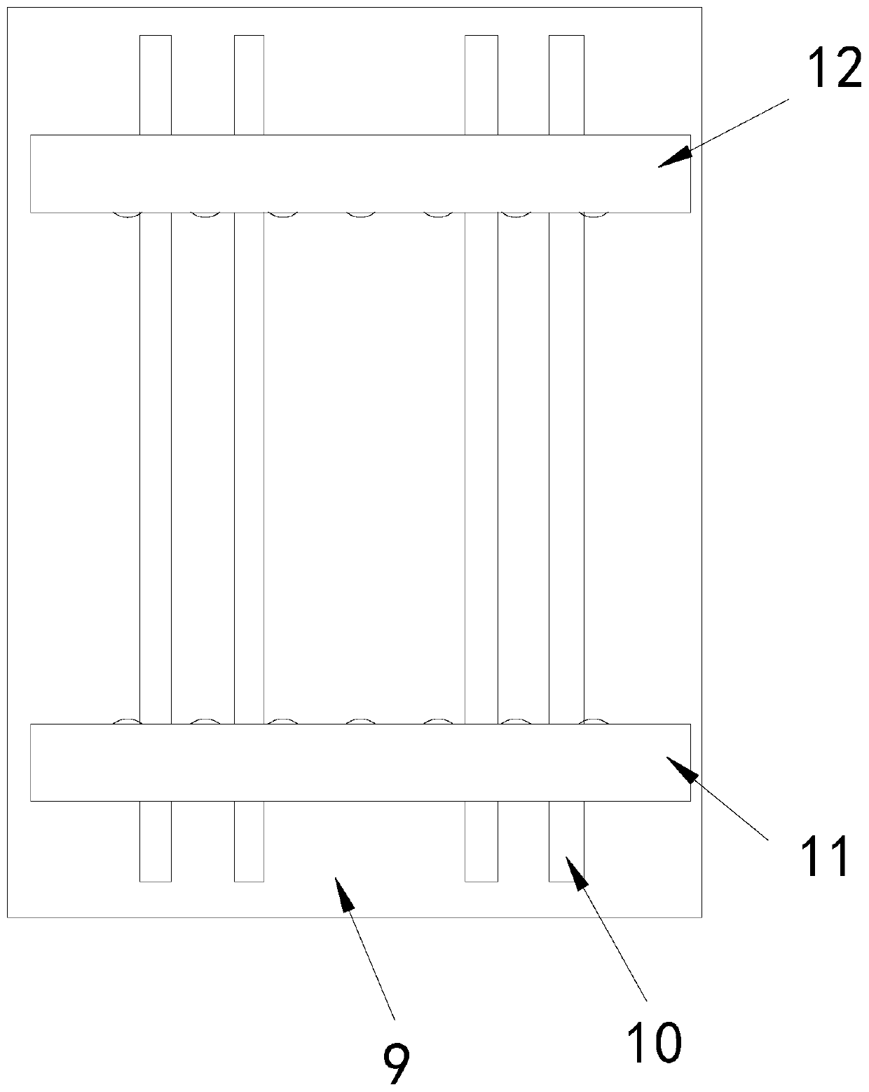
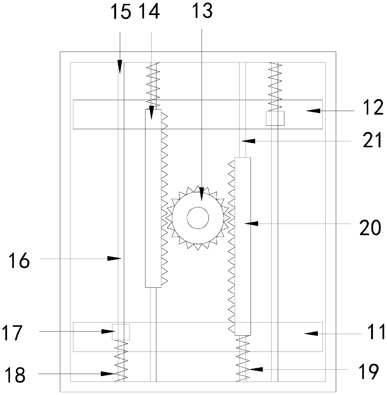
[0025] see Figure 1-5 , the present invention provides a technical scheme of tin spotting equipment for printed circuit board processing: its structure includes a base 1, a sliding table 2, a column 3, a tin supply system 4, a slider 5, a slide rail 6, a tin spray head 7, and a fixture 8. A sliding table 2 is installed on the base 1, and a fixture 8 is provided on the sliding table 2. Columns 3 are respectively connected to both sides of the base 1, and the t...


PUM


Abstract

The invention discloses a tin device for processing printed circuit boards. The structure of the tin device comprises a base, a sliding workbench, stand columns, a tin supply system, a slider, a sliderail, a tin spraying head and a clamp, the sliding workbench is mounted on the base, a clamp is arranged on the sliding workbench, the two sides of the base are respectively connected with the standcolumns, the top of the stand columns are connected with the slide rail, the slide rail is in sliding connection with the slider, the slider is connected with the tin spraying head, the tin spraying head is connected with the tin supply system, the tin supply system is arranged on the side surface of the stand column, the clamp comprises a protective base, a moving device, a first clamping plate and a second clamping plate, a moving device is arranged in the protective base, the first clamping plate and the second clamping plate are parallel to each other and are arranged on the protective base, the moving device is connected with the first clamping plate and the second clamping plate respectively. The tin device has the benefit effect that the double-panel type printed circuit board is clamped and fixed through the hourglass-shaped pulley, the circuit board can be kept in a horizontal state, soldering is facilitated better, and tilting is prevented.

Description

technical field [0001] The invention relates to the field of circuit boards, in particular to a tin spotting device for processing printed circuit boards. Background technique [0002] The copper foil of the copper-clad soldering board of the printed circuit board is very thin, and its electrical and thermal conductivity and covering properties are very poor. It is sufficient for low-power components, but it is not enough for high-power components. In order to make these pins The welding wire can conduct heat stably and has good adhesion. There are more tin points on the surface, and after wave soldering, it is made to be tinned in many places, which increases the strength, conduction, and thermal conductivity. [0003] Printed circuit boards are divided into single-sided boards, double-sided boards and multi-layer boards. When soldering, it is generally necessary to keep the circuit boards on a horizontal plane. Since both sides of the double-sided boards have structures, i...

Claims


Application Information

Patent Timeline
IPC IPC(8): B23K3/00B23K3/06B23K3/08B23K37/04
CPCB23K3/00B23K3/0607B23K3/087B23K2101/42
Inventor 陈强
Owner 陈强
Why Eureka
Try Eureka