
High-density wiring reset method

A reset method and high-density technology, applied in the manufacturing of electrical components, electrical solid-state devices, semiconductor/solid-state devices, etc., can solve the problems of sample failure, PAD pads can not be printed, deformation, etc., to improve the analysis speed and shorten the analysis. effect of cycles

Active Publication Date: 2020-01-24
闳康技术检测(上海)有限公司
View PDF5 Cites 2 Cited by
  • Summary
  • Abstract
  • Description
  • Claims
  • Application Information

AI Technical Summary

Problems solved by technology

[0003] The currently known technology needs to take the chip and repackage it. In this way, when bonding a chip with more than 20 wires, due to the excessive volume and number of wires on the chip, some of the wires on the chip will be crushed or severely deformed, and some parts will appear. The problem that the PAD pad cannot be connected online will cause the entire sample to fail

Method used


Image

  • High-density wiring reset method
  • High-density wiring reset method
  • High-density wiring reset method

Examples


Embodiment

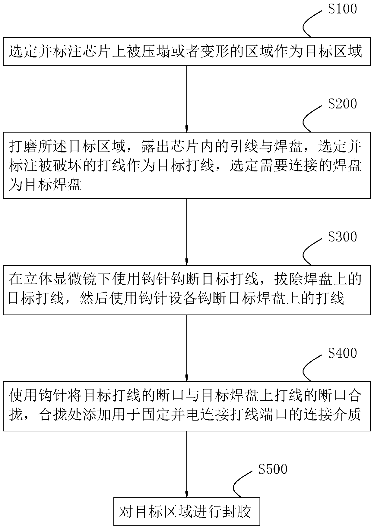
[0035] A high-density wiring reset method, such as figure 1 shown, including the following steps:

[0036] Step S100: Select and mark the crushed or deformed area on the chip as the target area. A pen can be used to draw a circle on the package of the chip.

[0037] Step S200: Polishing the target area to expose the leads and pads in the chip, selecting and marking the damaged bonding wires as the target bonding wires, and selecting the bonding pads to be connected as the target bonding pads. Use a grinder to grind the target area until the chip circuit in the package is exposed without damaging the internal circuit of the chip. Among them, the pads and wires are exposed. Target wires and target pads can be marked with a thin, colored pen.

[0038] Step S300 : use a crochet hook to cut off the target bonding wire under a stereo microscope, pull out the target bonding wire on the pad, and then use a crochet device to hook off the target bonding wire on the pad. The inner e...


PUM


Abstract

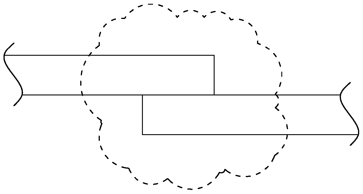
The invention relates to the technical field of semiconductor wiring, and discloses a high-density wiring reset method which comprises the following steps: S100, selecting and marking a collapsed or deformed area on a chip as a target area; S200, polishing the target area to expose the lead and the pad in the chip, selecting and marking the damaged wiring as the target wiring and selecting the padto be connected as the target pad; S300: using a crochet to hook off the target wiring under a stereo microscope, pulling out the target wiring on the pad and using crochet equipment to hook off thewiring on the target pad; S400: closing the fracture of the target wiring and the fracture of the wiring on the target pad and adding a connection medium for fixing and electrically connecting the wiring port at the closed place; and S500: sealing the target area. The wiring repair is directly performed on the chip and the analysis speed of the chip can be effectively improved through the wiring repair method without re-framing and wiring analysis from the packaging factory so as to shorten the analysis cycle of the chip.

Description

technical field [0001] The invention relates to semiconductor wire bonding, more specifically, it relates to a high-density wire bonding reset method. Background technique [0002] Wire bonding is also called WireBonding (pressure welding, also known as binding, bonding, wire bonding) refers to the use of metal wires (gold wires, aluminum wires, etc.), using thermal pressure or ultrasonic energy to complete the internal solid-state circuits in microelectronic devices. The connection of interconnection wires, that is, the connection between the chip and the circuit or lead frame, is common in the surface packaging process, such as the COB process. [0003] The currently known technology needs to take the chip and repackage it. In this way, when bonding a chip with more than 20 wires, due to the excessive volume of the chip and the number of wires, some of the wires on the chip will be crushed or severely deformed, and some parts will appear. The problem that the PAD pad cann...

Claims


Application Information

Patent Timeline
Patent Type & Authority Applications(China)
IPC IPC(8): H01L21/60
CPCH01L24/85H01L2224/85007H01L2224/85986
Inventor 高峰戴伟峰
Owner 闳康技术检测(上海)有限公司
Learn More