

Manufacturing method of nano structure
A nanostructure and fabrication method technology, applied in the field of nanostructure fabrication, can solve the problems of nanostructure damage, electron beam resist being difficult to be stripped off, etc.
- Summary
- Abstract
- Description
- Claims
- Application Information
AI Technical Summary
Problems solved by technology
Method used
Image

Examples
Embodiment 1
[0075] The manufacturing process of the nanostructure of the present embodiment is specifically as follows:
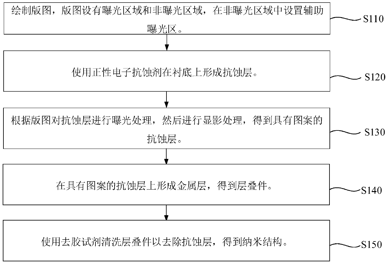
[0076] (1) Use L-Edit software to draw the layout according to the graph of the nanostructure, wherein the layout is provided with an exposure area and a non-exposure area, and 3 auxiliary exposure areas are set in the non-exposure area, and the 3 auxiliary exposure areas are arranged along a straight line, And the auxiliary exposure area is located in the middle of the non-exposed area, and the ratio of the total area of the three auxiliary exposure areas to the area of the non-exposed area is 1:4.
[0077] (2) Use polymethyl methacrylate as the positive electronic resist, and use a glue coater to spin-coat the positive electronic resist on the substrate to form a resist layer with a thickness of 200 nanometers.
[0078] (3) Expose the resist layer according to the layout, and then use a developer to develop it for 2 minutes to obtain a resist layer with a pattern...
Embodiment 2
[0082] The manufacturing process of the nanostructure of the present embodiment is specifically as follows:
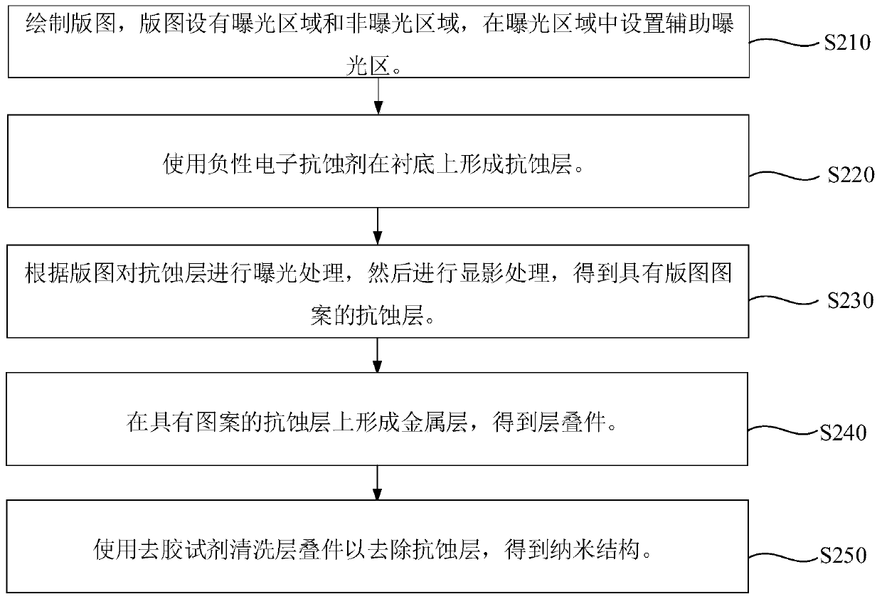
[0083] (1) Use L-Edit software to draw the layout according to the graph of the nanostructure, wherein the layout is provided with an exposure area and a non-exposure area, 2 auxiliary exposure areas are set in the non-exposure area, and 2 auxiliary exposure intervals are set, and the auxiliary The exposed area is located in the middle of the non-exposed area, and the ratio of the total area of the two auxiliary exposed areas to the area of the non-exposed area is 1:7.
[0084] (2) Use polymethyl methacrylate as the positive electronic resist, and use a coating machine to spin-coat the positive electronic resist on the substrate to form a resist layer with a thickness of 100 nanometers.
[0085] (3) Expose the resist layer according to the layout, and then use a developer to develop it for 1 minute to obtain a resist layer with a pattern. Among them, the exposure ...
Embodiment 3
[0089] The manufacturing process of the nanostructure of the present embodiment is specifically as follows:
[0090] (1) Use L-Edit software to draw the layout according to the graph of the nanostructure, wherein the layout is provided with an exposure area and a non-exposure area, and 6 auxiliary exposure areas are set in the non-exposure area, and the 6 auxiliary exposure areas are along an arc set, and the auxiliary exposure area is located in the middle of the non-exposed area, the ratio of the total area of the six auxiliary exposure areas to the area of the non-exposed area is 1:30.
[0091] (2) Use polymethyl methacrylate as the positive electronic resist, and use a glue coater to spin-coat the positive electronic resist on the substrate to form a resist layer with a thickness of 300 nanometers.
[0092] (3) Expose the resist layer according to the layout, and then use a developer to develop it for 3 minutes to obtain a resist layer with a pattern. Among them, the ex...
PUM
| Property | Measurement | Unit |
|---|---|---|
| thickness | aaaaa | aaaaa |
| thickness | aaaaa | aaaaa |
| thickness | aaaaa | aaaaa |
Abstract
Description
Claims
Application Information