Method for preparing material with highly gradient surface micronano structure

A technology of micro-nano structure and target material, applied in the field of nano-material processing, to achieve the effects of high time consumption, high controllability and repeatability, and simple operation

Inactive Publication Date: 2013-03-20
PEKING UNIV
View PDF3 Cites 0 Cited by
  • Summary
  • Abstract
  • Description
  • Claims
  • Application Information

AI Technical Summary

Problems solved by technology

However, these methods are difficult to construct an ideal structure with a high degree of gradient and a smooth surface.

Method used


Image

  • Method for preparing material with highly gradient surface micronano structure
  • Method for preparing material with highly gradient surface micronano structure
  • Method for preparing material with highly gradient surface micronano structure

Examples


Embodiment 1

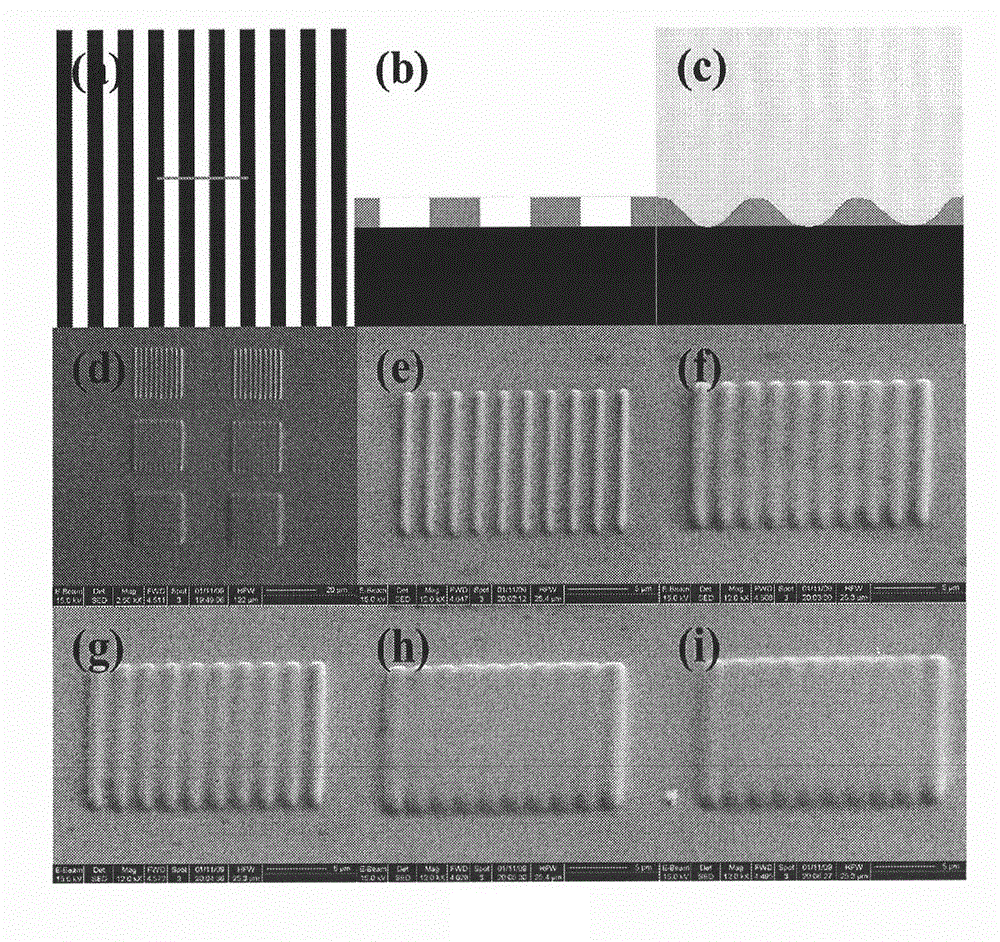
[0037] Example 1. Preparation of materials with wavy structure on the surface

[0038] 1) Coat PMMA on the Si substrate to obtain an electronic resist layer, and bake the glue at 170°C (heating rate of 20°C / min) for 30 minutes;

[0039] 2) Expose the PMMA layer that has been baked in the step 1) with electron beams, develop with a developer solution of methyl isobutyl ketone (MIBK): isobutanol = 1:3, and rinse with alcohol for fixing; the resulting pattern Such as figure 1 As shown in (a), the exposure pattern is a black area; figure 1 The exposure pattern of (b) is figure 1 (a) A cross-sectional view of the PMMA structure after exposure of the black short line indicates the area, wherein the lower part of the cross-sectional view is the silicon substrate, and the upper part is PMMA.

[0040] 3) On the electronic resist layer that has been fixed in step 2), coat anisole when the rotation speed of the spinner reaches 3000 rpm, and heat it at 170°C (heating rate is 20°C / min) 30min und...

Embodiment 2

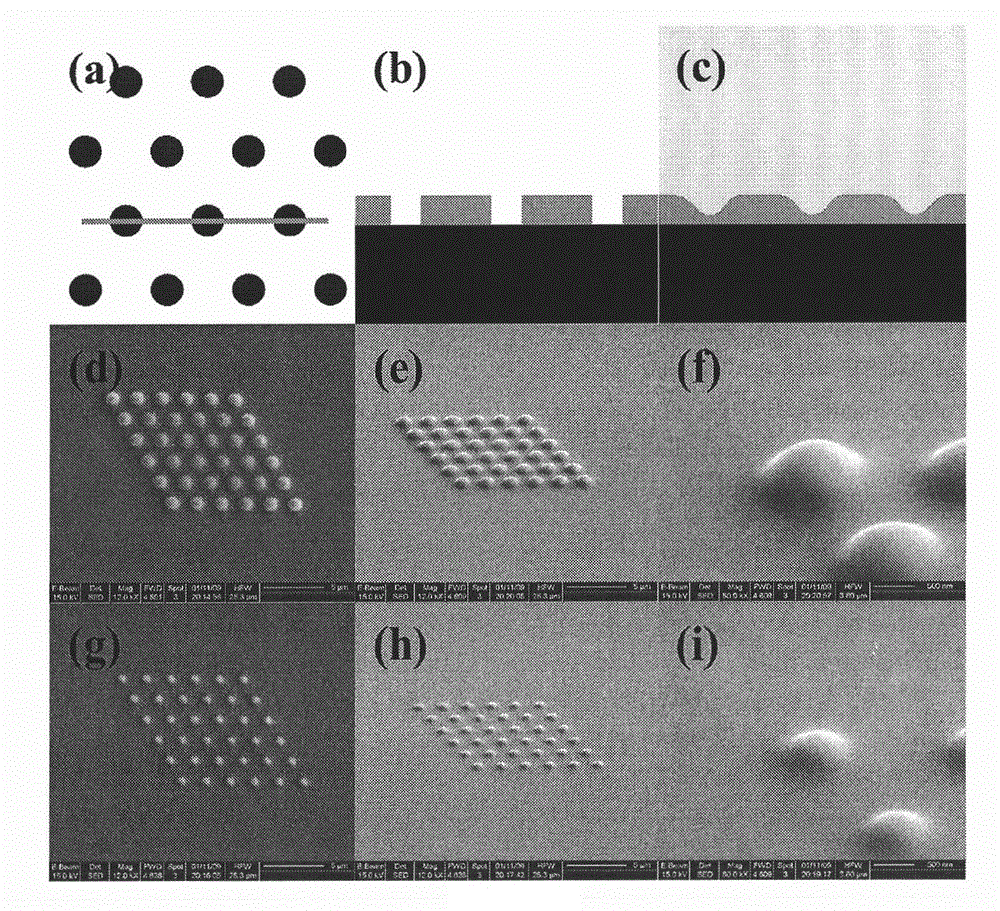
[0047] Example 2. Preparation of a material with a smooth protrusion structure on the surface

[0048] 1) Coat PMMA on the Si substrate to obtain an electronic resist layer, and bake the glue at 170°C (heating rate of 20°C / min) for 30 minutes;

[0049] 2) Expose the PMMA layer that has been baked in the step 1) with electron beams, develop with a developer solution of methyl isobutyl ketone (MIBK): isobutanol = 1:3, and rinse with alcohol for fixing; the resulting pattern Such as figure 2 As shown in (a), the exposure pattern is a blue area; figure 2 The exposure pattern of (b) is figure 2 (a) A cross-sectional view of the PMMA structure after exposure of the black short line indicates the area, wherein the lower part of the cross-sectional view is the silicon substrate, and the upper part is PMMA.

[0050] 3) On the electronic resist layer that has been fixed in step 2), coat anisole when the rotation speed of the spinner reaches 3000 rpm, and heat it at 170°C (heating rate is 20...

Embodiment 3

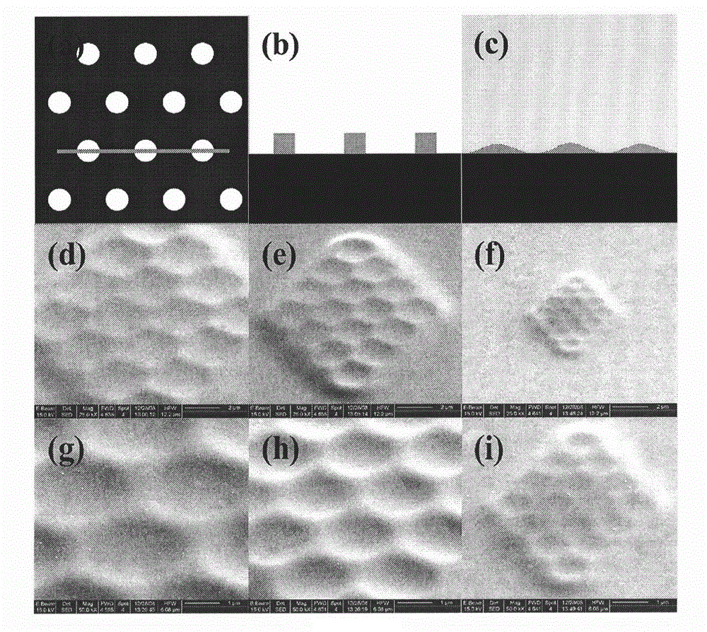
[0057] Embodiment 3. Preparation of a material with a smooth concave array structure on the surface

[0058] 1) Coat PMMA on the Si substrate to obtain an electronic resist layer, and bake the glue at 170°C (heating rate of 20°C / min) for 30 minutes;

[0059] 2) Expose the PMMA layer that has been baked in the step 1) with electron beams, develop with a developer solution of methyl isobutyl ketone (MIBK): isobutanol = 1:3, and rinse with alcohol for fixing; the resulting pattern Such as image 3 As shown in (a), the exposure pattern is a blue area; image 3 The exposure pattern of (b) is image 3 (a) A cross-sectional view of the PMMA structure after exposure of the black short line indicates the area, wherein the lower part of the cross-sectional view is the silicon substrate and the upper part is PMMA.

[0060] 3) On the electronic resist layer that has been fixed in step 2), coat anisole when the rotation speed of the spinner reaches 3000 rpm, and heat it at 170°C (heating rate is ...


PUM


Abstract

The invention discloses a method for preparing a material with a highly gradient surface micronano structure. The method comprises the following steps of: 1) coating an electron beam resist on a substrate to obtain an electron beam resist layer, and baking the electron beam resist layer ; 2) exposing, developing and fixing electron beams; 3) coating anisole to obtain an anisole layer, and baking the anisole layer; 4) depositing a target material on the anisole layer to obtain a target material layer; 5) attaching the target material layer to another substrate; and 6) separating the target material layer from the electron beam resist layer. The method has the advantages of simple and convenient operation mode, wide material application range, customized shape and position of a pattern, smooth structural surface and high controllability and repeatability, and can play an important role in fields of surface plasmon research, self assembly of nano particles, utilization of solar energy, micro-flow research and the like.

Description

Technical field [0001] The invention relates to the field of nano-material processing, and relates to a method for preparing a material with a micro-nano structure, in particular to a method for preparing a material with a surface micro-nano structure. Background technique [0002] The structure of surface micro and nanostructures is of great significance in many fields, and has played a huge role in aspects including surface plasmons, self-assembly of nanoparticles, solar energy utilization, and microfluidic devices (H. Ditlbacher, JRKrenn, G. Schider et al. Applied Physics Letters, 81, 1762 (2002); MJ Lee, J. Kim and YSNanotechnology, 19, 355301 (2008); A. Lasagni, M. Nejati, R. Clasen et al. Advanced Functional Materials, 8, 580 (2006); S. Billat, K. Kliche, R. Gronmaier et al. Sensors and Actuators A: Physical, 145-146, 66 (2008)). Along with the trend of device miniaturization, diversified micro and nano processing methods have been greatly developed, so as to obtain simple...

Claims


Application Information

Patent Timeline
Patent Type & Authority Patents(China)
IPC IPC(8): B82B3/00
Inventor 张洋朱新利俞大鹏
Owner PEKING UNIV
Why Eureka
Try Eureka