System on chip and FPGA kernel information processing method thereof

A system-on-chip and core technology, applied in electrical digital data processing, architecture with a single central processing unit, CAD circuit design, etc., can solve the problems of interconnection communication, reduced wiring efficiency, unbalanced wiring resources, etc., to improve wiring Efficiency, reduce chip power consumption, improve the effect of interconnect timing

Active Publication Date: 2020-01-31
GOWIN SEMICON CORP LTD
View PDF6 Cites 11 Cited by
  • Summary
  • Abstract
  • Description
  • Claims
  • Application Information

AI Technical Summary

Problems solved by technology

[0002] At present, as the semiconductor industry enters the era of ultra-deep submicron and even nanometer processing, it is an inevitable development trend to realize a complex electronic system on a single integrated circuit core. SoC (System on Chip, system on chip) is becoming more and more widely used. Application, in the prior art, the system on chip is the FPGA (Field-Programmable Gate Array, Field Programmable Gate Array) core that connects the MCU (Microcontroller Unit, single-chip microcomputer) core, memory, external devices, etc., and then leads to the bus (the public communication trunk line for transmitting information between different devices), and the bus wiring will be carried out inside the FPGA core. Due to the limitations of the gate array arrangement, software model layout, and on-chip area of ​​the FPGA core, the length of the on-chip wiring of the core will be caused. Unbalanced wiring resources and other issues, resulting in timing and power consumption that cannot fully meet the interconnection and communication between the cores of the MCU core and the FPGA core, and the MCU cores of different architectures need to manually identify the bus information and input it to the wiring software. Easy to enter mistakes and reduce wiring efficiency

Method used


Image

  • System on chip and FPGA kernel information processing method thereof
  • System on chip and FPGA kernel information processing method thereof
  • System on chip and FPGA kernel information processing method thereof

Examples


Embodiment Construction

[0017] The following will clearly and completely describe the technical solutions in the embodiments of the present invention with reference to the accompanying drawings in the embodiments of the present invention. Obviously, the described embodiments are some of the embodiments of the present invention, but not all of them. Based on the embodiments of the present invention, all other embodiments obtained by persons of ordinary skill in the art without creative efforts fall within the protection scope of the present invention.

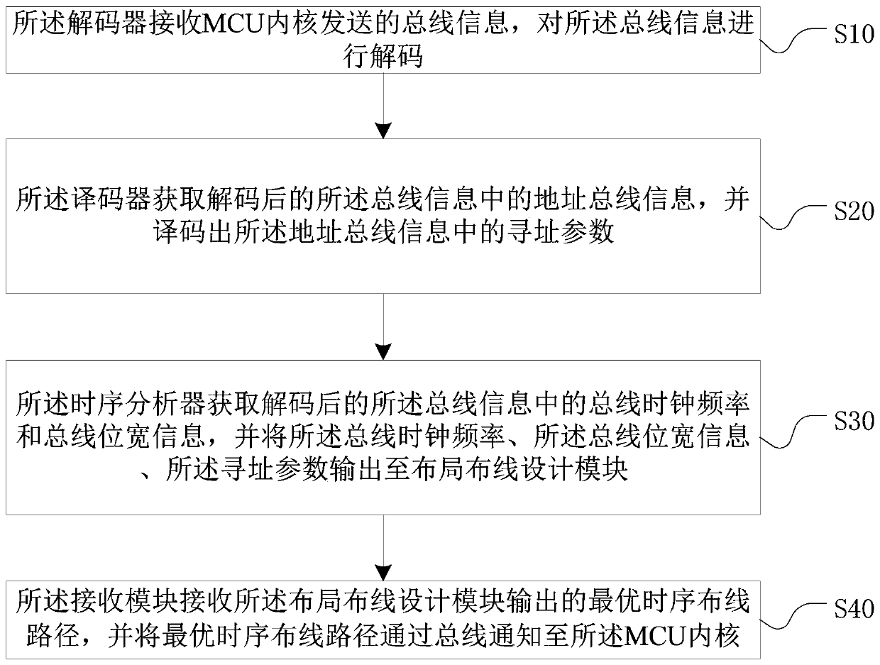
[0018] The present invention provides a system on chip 1, by automatically identifying the bus information of the MCU core 2 to output the optimal timing wiring path of the FPGA core 3 that matches the MCU core 2, and performing wiring according to the optimal timing wiring path, thereby improving the wiring efficiency. Therefore, the interconnection timing between the MCU core 2 and the FPGA core 3 is improved, the power consumption of the chip is redu...


PUM


Abstract

The invention discloses a system on chip and an FPGA kernel information processing method thereof. The method comprises the steps of decoding bus information sent by an MCU kernel; decoding addressingparameters in the address bus information; acquiring bus clock frequency and bus bit width information in the decoded bus information, and outputting the acquired bus clock frequency, bus bit width information and addressing parameters to a layout wiring design module; and notifying the optimal time sequence wiring path output by the layout wiring design module to the MCU core through the bus. According to the invention, the optimal time sequence wiring path of the FPGA core matched with the MCU core is output by automatically identifying the bus information of the MCU core; wiring is carriedout according to the optimal timing sequence wiring path, so that the wiring efficiency is improved, the interconnection timing sequence of the MCU core and the FPGA core is improved, the chip powerconsumption is reduced, and the performance requirement of interconnection communication of the MCU core and the FPGA core is met.

Description

technical field [0001] The invention relates to the technical field of semiconductor chips, in particular to a system on chip and an FPGA kernel information processing method thereof. Background technique [0002] At present, as the semiconductor industry enters the era of ultra-deep submicron and even nanometer processing, it is an inevitable development trend to realize a complex electronic system on a single integrated circuit core. SoC (System on Chip, system on chip) is becoming more and more widely used. Application, in the prior art, the system on chip is the FPGA (Field-Programmable Gate Array, Field Programmable Gate Array) core that connects the MCU (Microcontroller Unit, single-chip microcomputer) core, memory, external devices, etc., and then leads to the bus (the public communication trunk line for transmitting information between different devices), and the bus wiring will be carried out inside the FPGA core. Due to the limitations of the gate array arrangement...

Claims


Application Information

Patent Timeline
Patent Type & Authority Applications(China)
IPC IPC(8): G06F30/34G06F15/78
CPCG06F15/7807
Inventor 王铜铜刘锴马得尧范召杜金凤
Owner GOWIN SEMICON CORP LTD
Why Eureka
Try Eureka