Light wave mode conversion device and manufacturing method thereof

A technology of mode conversion and manufacturing method, applied in the direction of optical waveguide and light guide, can solve the problem of low optical coupling efficiency of optical waveguide, and achieve the effect of reducing process complexity, improving coupling efficiency, and low-loss interconnection

Inactive Publication Date: 2020-02-04
SHANGHAI IND U TECH RES INST
View PDF5 Cites 2 Cited by
  • Summary
  • Abstract
  • Description
  • Claims
  • Application Information

AI Technical Summary

Problems solved by technology

[0006] The present invention provides a light wave mode conversion device and its manufacturing method to solve the problem of low optical coupling efficiency between existing light waveguides with different mode fields

Method used


Image

  • Light wave mode conversion device and manufacturing method thereof
  • Light wave mode conversion device and manufacturing method thereof
  • Light wave mode conversion device and manufacturing method thereof

Examples


Embodiment Construction

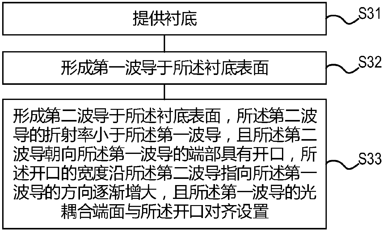
[0028] The specific implementation of the optical wave mode conversion device and its manufacturing method provided by the present invention will be described in detail below with reference to the accompanying drawings.

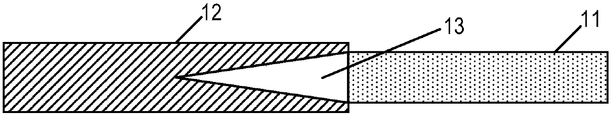
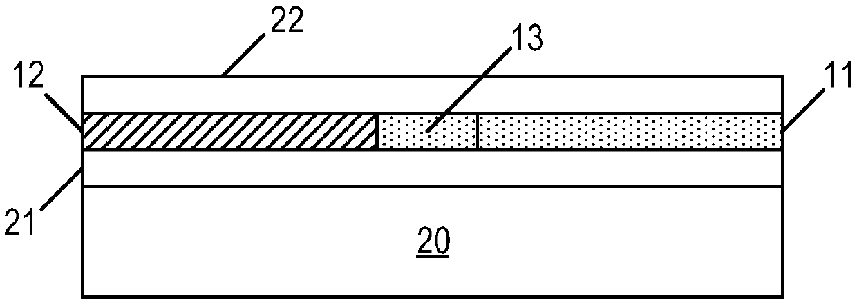
[0029] This specific embodiment provides a light wave mode conversion device, with figure 1 It is a schematic diagram of the top view structure of the light wave mode conversion device in the specific embodiment of the present invention, with figure 2 It is a schematic cross-sectional structure diagram of a light wave mode conversion device in a specific embodiment of the present invention.

[0030] Such as figure 1 , figure 2 As shown, the optical wave mode conversion device provided in this specific embodiment includes a first waveguide 11 and a second waveguide 12 arranged in the same layer, and the refractive index of the first waveguide 11 is greater than that of the second waveguide 12; The end of the second waveguide 12 facing the first waveguide ...


PUM


Abstract

The invention relates to the technical field of semiconductors, and in particular relates to a light wave mode conversion device and a manufacturing method thereof. The light wave mode conversion device comprises a first waveguide and a second waveguide, which are arranged in the same layer; furthermore, the refractive index of the first waveguide is greater than that of the second waveguide; theend part, towards the first waveguide, of the second waveguide is provided with an opening; the diameter of the opening is gradually increased in the direction from the second waveguide to the first waveguide; and furthermore, and the light coupling end face of the first waveguide and the opening are arranged to be aligned. By means of the light wave mode conversion device and the manufacturing method thereof in the invention, the process complexity of an optical device is reduced; furthermore, the coupling efficiency between the two waveguides is increased; and, low-loss interconnection between the two waveguides is realized.

Description

technical field [0001] The invention relates to the technical field of semiconductors, in particular to a light wave mode conversion device and a manufacturing method thereof. Background technique [0002] With the upgrading of network products, the size and power consumption of modules used in the network are constantly decreasing to meet the needs of continuous cost reduction and performance improvement. Due to its unique characteristics such as low cost, ultra-small size, and low power consumption, silicon-based photonic devices have attracted extensive attention from the industry in recent years, and have become one of the key considerations in the upgrading of network products. [0003] In the prior art, due to the characteristics of low nonlinearity, allowing greater energy input, and lower transmission loss, the silicon nitride waveguide has natural advantages in the input requiring greater energy. However, the nature of the silicon nitride material determines that i...

Claims


Application Information

Patent Timeline
Patent Type & Authority Applications(China)
IPC IPC(8): G02B6/14G02B6/13
CPCG02B6/13G02B6/14
Inventor 王庆方青汪巍涂芝娟曾友宏蔡艳王书晓余明斌
Owner SHANGHAI IND U TECH RES INST
Why Eureka
Try Eureka