Back capacitor structure and manufacturing method

A capacitor structure and manufacturing method technology, which is applied in the direction of capacitors, circuits, electrical components, etc., can solve the problems of large area of ​​semiconductor devices, achieve the effects of increasing capacitor area, improving area utilization, and saving process costs

Active Publication Date: 2020-02-04
福建省福联集成电路有限公司
View PDF7 Cites 2 Cited by
  • Summary
  • Abstract
  • Description
  • Claims
  • Application Information

AI Technical Summary

Problems solved by technology

[0003] Therefore, it is necessary to provide a backside capacitor structure and manufacturing method to solve the problem that traditional planar capacitors occupy a large area of ​​semiconductor devices

Method used


Image

  • Back capacitor structure and manufacturing method
  • Back capacitor structure and manufacturing method
  • Back capacitor structure and manufacturing method

Examples


Embodiment Construction

[0049] In order to explain in detail the technical content, structural features, achieved goals and effects of the technical solution, the following will be described in detail in conjunction with specific embodiments and accompanying drawings.

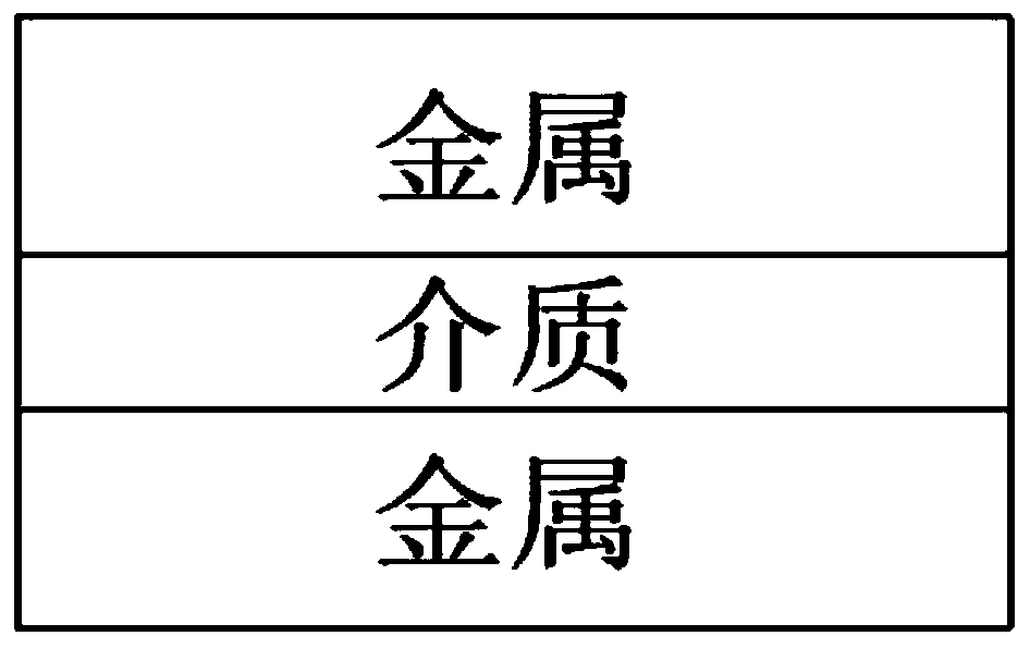
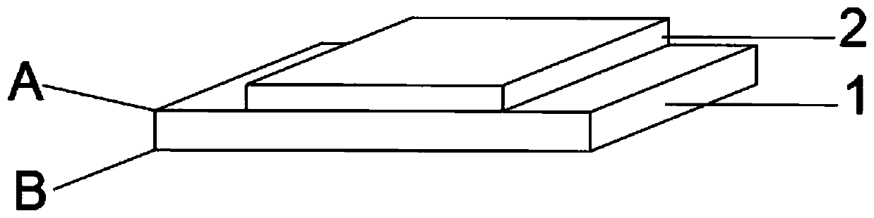
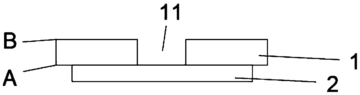
[0050] see Figure 2 to Figure 9 This embodiment provides a method for manufacturing a backside capacitor. The method can be performed on a semiconductor substrate, such as a wafer or a chip, and the semiconductor substrate is a gallium arsenide substrate or a silicon substrate. Many components and devices are fabricated on the front side A of the semiconductor device substrate 1. In order to reduce the occupation of the capacitor structure on the front side A, after the device protection on the front side A of the substrate 1 is completed, it is turned to the back side B of the substrate 1. The back side B of the bottom carries out the making of hole 11. It includes the following steps: depositing a nitride layer 2 on the front side...


PUM


Abstract

The invention discloses a back capacitor structure and a manufacturing method. The method comprises the following steps of arranging a nitride layer on the front of a semiconductor substrate and arranging a hole, directly facing the nitride layer, in the back of the semiconductor substrate, wherein the nitride layer is arranged at the bottom of the hole; arranging first metal layers on the inner wall of the hole and the back of the semiconductor substrate; arranging dielectric layers on the inner wall of the hole and the back of the semiconductor substrate, wherein the dielectric layers coverthe first metal layers; arranging through holes in the dielectric layer above the first metal layers of the semiconductor substrate; and manufacturing a hole in the back of the semiconductor substrate. The capacitor structure in the manufactured hole is capable of greatly improving the capacity area, thereby improving the area utilization rate of an epitaxy structure; the occupied planar space issmaller, so that benefit is provided to reduce the device size; and the back capacitor is manufactured without changing the original manufacturing process, so that the process cost is saved.

Description

technical field [0001] The invention relates to the field of manufacturing capacitors on semiconductor devices, in particular to a back capacitor structure and a manufacturing method. Background technique [0002] The production of capacitors is formed by the first metal layer and the second metal layer and the medium between them. The structure is as follows: figure 1 shown. Generally, passive component capacitors are fabricated on the front side of semiconductor devices. In order to save the area of ​​semiconductor devices, the traditional planar capacitor structure has a lower area S and a lower capacitance value. In general, once the material of the dielectric layer is determined, the minimum spacing is determined. To increase the capacitance, the area of ​​the plate is generally increased, but this greatly occupies the chip area, which is not conducive to integration. Contents of the invention [0003] For this reason, it is necessary to provide a back capacitor str...

Claims


Application Information

Patent Timeline
Patent Type & Authority Applications(China)
IPC IPC(8): H01L23/64
CPCH01L28/40H01L28/90H01L28/91
Inventor 吴淑芳陈智广李立中黄光伟吴靖马跃辉庄永淳林伟铭
Owner 福建省福联集成电路有限公司
Why Eureka
Try Eureka