Display substrate, preparation method thereof, and display device

A technology for display substrates and substrates, used in semiconductor/solid-state device manufacturing, electrical components, electrical solid-state devices, etc., can solve problems such as increased production costs, save production costs, reduce process processes, and prevent adverse effects.

Active Publication Date: 2020-02-04
BOE TECH GRP CO LTD +1
View PDF6 Cites 1 Cited by
  • Summary
  • Abstract
  • Description
  • Claims
  • Application Information

AI Technical Summary

Problems solved by technology

[0004] The technical problem to be solved in this application is to solve the problem of increased production cost due to the use of UV masks in the process of display substrate preparation

Method used


Image

  • Display substrate, preparation method thereof, and display device
  • Display substrate, preparation method thereof, and display device
  • Display substrate, preparation method thereof, and display device

Examples


Embodiment Construction

[0040] The technical solution of the present application will be further described below in conjunction with the accompanying drawings and through specific implementation methods. It should be understood that the specific embodiments described here are only used to explain the present application, but not to limit the present application.

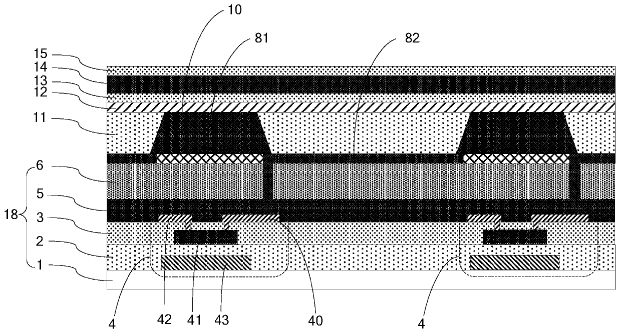
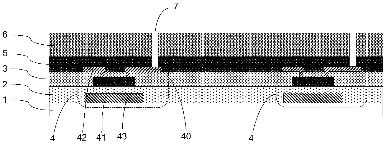
[0041] figure 1 It is a schematic structural diagram of a display substrate according to an embodiment of the present application, such as figure 1 As shown, the display substrate of this embodiment includes: a driving structure layer 18 and a light emitting structure layer stacked on the substrate 1, the driving structure layer 18 includes a thin film transistor 4, and the light emitting structure layer includes a first electrode 82 and a light emitting structure layer. The shielding layer 81 for shielding ultraviolet light, the orthographic projection of the shielding layer 81 on the substrate 1 includes the orthographic projection of th...


PUM

PropertyMeasurementUnit
thicknessaaaaaaaaaa
electrical resistivityaaaaaaaaaa
transmittivityaaaaaaaaaa

Abstract

The invention provides a display substrate, a preparation method thereof, and a display device, and relates to the technical field of display devices. The display substrate comprises a driving structure layer and a light-emitting structure layer which are arranged on a base in an overlapped mode, the driving structure layer comprises a thin film transistor, the light-emitting structure layer comprises a first electrode and a shielding layer used for shielding ultraviolet light (UV), and the front projection of the shielding layer on the base contains the front projection of the thin film transistor on the base. According to the display substrate in the embodiment of the invention, the problem that in the preparation process of the display substrate, a UV mask plate is adopted, and consequently, the production cost is increased can be solved.

Description

technical field [0001] The present application relates to the technical field of display devices, in particular to a display substrate, a manufacturing method thereof, and a display device. Background technique [0002] Organic light-emitting diodes (OLEDs) have gradually developed in the fields of display and lighting technologies in recent years, especially in the field of display, because of their advantages such as high response, high contrast, and flexibility, they have broad application prospects. However, because OLED devices will be corroded and damaged under the action of water vapor and oxygen, it is particularly important to choose a better packaging method for OLED devices. At present, the thin-film encapsulation method for the display substrate is usually to cover the OLED device with a thin-film encapsulation structure stacked with inorganic layers and organic layers, so as to achieve the purpose of blocking water and oxygen. Among them, the inorganic layer is...

Claims


Application Information

Patent Timeline
Patent Type & Authority Applications(China)
IPC IPC(8): H01L27/32H01L51/56
CPCH10K59/12H10K59/126H10K71/00
Inventor 宫奎段献学张志海刘天真
Owner BOE TECH GRP CO LTD
Why Eureka
Try Eureka