

Silicon-based adapter plate structure for reducing equivalent dielectric constant and preparation method thereof
A technology of equivalent dielectric constant and low dielectric constant materials, applied in circuits, electrical components, electric solid devices, etc., can solve the problems of high cost, long period, large transmission delay, etc.
- Summary
- Abstract
- Description
- Claims
- Application Information
AI Technical Summary
Problems solved by technology
Method used
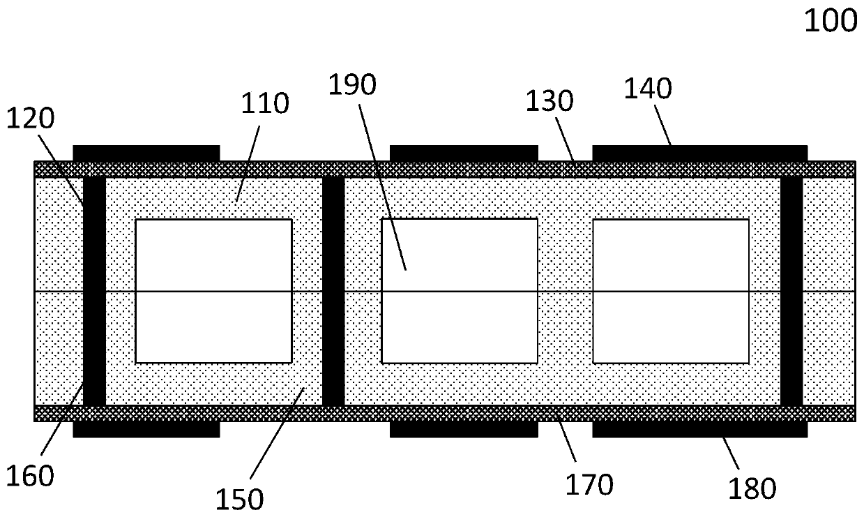
Image

Examples
Embodiment Construction
[0044] In the following description, the present invention is described with reference to various examples. One skilled in the art will recognize, however, that the various embodiments may be practiced without one or more of the specific details, or with other alternative and / or additional methods, materials, or components. In other instances, well-known structures, materials, or operations are not shown or described in detail so as not to obscure aspects of the various embodiments of the invention. Similarly, for purposes of explanation, specific quantities, materials and configurations are set forth in order to provide a thorough understanding of embodiments of the invention. However, the invention may be practiced without these specific details. Furthermore, it should be understood that the various embodiments shown in the drawings are illustrative representations and are not necessarily drawn to scale.
[0045] In this specification, reference to "one embodiment" or "the...
PUM
| Property | Measurement | Unit |
|---|---|---|
| thickness | aaaaa | aaaaa |
Abstract
Description
Claims
Application Information