Display panel, manufacturing method thereof, and display device

A display panel and display area technology, applied in semiconductor/solid-state device manufacturing, semiconductor devices, electrical components, etc., can solve problems affecting OLED life, inorganic packaging layer damage, packaging failure, etc., to ensure life, avoid packaging failure, Guarantee the effect of encapsulation effect

Active Publication Date: 2022-05-20
BOE TECH GRP CO LTD
View PDF6 Cites 0 Cited by
  • Summary
  • Abstract
  • Description
  • Claims
  • Application Information

AI Technical Summary

Problems solved by technology

[0005] In the existing technology, such as figure 1 as shown, figure 1 It is a schematic diagram of the packaging area of ​​a display panel. Since the angle θ of the foot of the isolation column in the inverted trapezoidal structure is small, the thickness of the inorganic packaging layer at the foot of the isolation column is relatively thin, so that the inorganic packaging layer is easy to be placed at the bottom of the isolation column. The position of the pin is damaged, causing the package to fail, making water and oxygen invade into the OLED through the isolation column, which affects the life of the OLED

Method used


Image

  • Display panel, manufacturing method thereof, and display device
  • Display panel, manufacturing method thereof, and display device
  • Display panel, manufacturing method thereof, and display device

Examples


no. 1 example

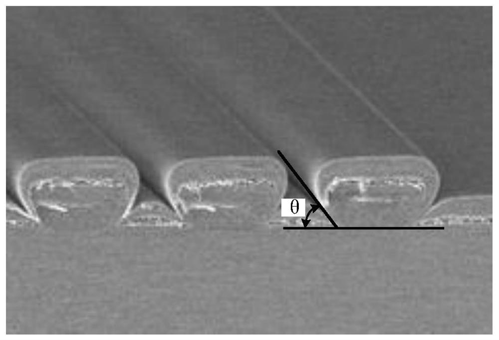
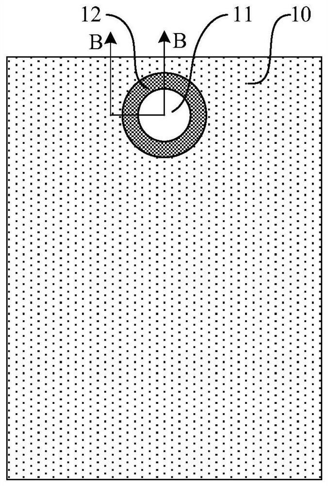
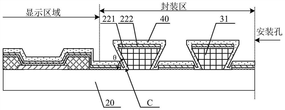
[0067] The schematic diagram of the planar structure of the display panel of the embodiment of the present invention is as follows: Figure 2a as shown, image 3 For the first embodiment of the present invention, the display panel is Figure 2a The B-B cross-sectional schematic diagram in, Figure 4 for image 3 An enlarged schematic view of part C in . The display panel of the embodiment of the present invention, such as Figure 2a with image 3 As shown, on a plane parallel to the display panel, the display panel includes a display area 10, and a mounting hole 11 is arranged in the display area 10, and a packaging area 12 between the display area 10 and the mounting hole 11 is arranged around the mounting hole 11. .

[0068] Such as image 3 As shown, on a plane perpendicular to the display panel, the structure of the packaging area includes an isolation structure 30 disposed on the base substrate 20 , and the isolation structure 30 is disposed around the mounting hol...

no. 2 example

[0110] Based on the technical idea of ​​the embodiment of the present invention, the embodiment of the present invention also proposes a method for manufacturing a display panel. The display panel includes a display area, a mounting hole located in the display area, and a packaging area disposed between the mounting hole and the display area, and the manufacturing method includes forming a An isolation structure, forming the isolation structure includes:

[0111] An isolation column on the base substrate is formed in the packaging area, and the orthographic projection of the side of the isolation column close to the base substrate on the base substrate is located at the side of the isolation column away from the base substrate. one side in an orthographic projection on the substrate substrate;

[0112] A smooth layer is formed in the packaging area, the smooth layer is located on both sides of the isolation column, the gentle layer includes a filling part in contact with the ...

no. 3 example

[0135] Based on the inventive concepts of the aforementioned embodiments, an embodiment of the present invention further provides a display device, which includes the display panel using the aforementioned embodiments. The display device can be any product or component with a display function such as a mobile phone, a tablet computer, a television, a monitor, a notebook computer, a digital photo frame, a navigator, and the like.


PUM

PropertyMeasurementUnit
thicknessaaaaaaaaaa
thicknessaaaaaaaaaa
quality scoreaaaaaaaaaa

Abstract

The invention discloses a display panel, a preparation method thereof, and a display device. The display panel includes a mounting hole and a packaging area surrounding the mounting hole, the packaging area includes a base substrate, an isolation structure disposed on the base substrate, the isolation structure includes an isolation column and behind the isolation column A gentle layer formed and located on both sides of the isolation column, the gentle layer includes a filling part in contact with the sidewall of the isolation column, and the surface of the filling part on the side facing away from the base substrate is far away from the isolation column. The post position gradually moves away from the base substrate toward the direction closer to the spacer post position. The display panel eliminates the sharp surface at the bottom of the side wall of the isolation column, making the bottom surface of the side wall of the isolation column more gentle, thereby making the film thickness of the inorganic packaging layer more uniform, avoiding packaging failure, ensuring the packaging effect, and ensuring The life of the OLED in the display area is greatly reduced.

Description

technical field [0001] The invention relates to the field of display technology, in particular to a display panel, a manufacturing method thereof, and a display device. Background technique [0002] Organic Light Emitting Diode (OLED) is an active light-emitting display device, which has the advantages of self-illumination, wide viewing angle, high contrast, low power consumption, and fast response. With the continuous development of display technology, OLED technology is increasingly used in various display devices, especially smart terminal products such as mobile phones and tablet computers. [0003] With the development of active matrix organic light-emitting diode (Active Matrix Organic Light-EmittintgDiode, AMOLED) technology, the requirements for the display area of ​​display devices are getting higher and higher, such as full screen and borderless screen, in order to bring users more Dazzling visual impact. Since products such as smart terminals usually need to be ...

Claims


Application Information

Patent Timeline
Patent Type & Authority Patents(China)
IPC IPC(8): H01L51/52H01L27/32H01L51/56
CPCH10K59/00H10K50/84H10K50/844H10K71/00
Inventor 弓浩然谢春燕韩子昂林新琦
Owner BOE TECH GRP CO LTD
Why Eureka
Try Eureka