Unlock instant, AI-driven research and patent intelligence for your innovation.

3D NAND manufacturing method and memory

A technology of 3D NAND and manufacturing method, which is applied in the direction of semiconductor devices, electric solid devices, electrical components, etc., can solve the problems such as structural instability cannot be guaranteed, and achieve the effect of more structure, enlarged opening area, and stable structure

Pending Publication Date: 2020-02-18
YANGTZE MEMORY TECH CO LTD
View PDF7 Cites 0 Cited by
  • Summary
  • Abstract
  • Description
  • Claims
  • Application Information

AI Technical Summary

Problems solved by technology

[0005] In view of this, the present invention provides a 3D NAND manufacturing method and memory to solve the problem in the prior art that the structural instability in the manufacturing process cannot be guaranteed due to the increase in the number of layers of the O / N stack structure in the 3D NAND flash memory.

Method used


Image

  • 3D NAND manufacturing method and memory
  • 3D NAND manufacturing method and memory
  • 3D NAND manufacturing method and memory

Examples


Embodiment Construction

[0038] As mentioned in the background technology section, in the prior art, as the number of layers of the O / N stack structure in the 3D NAND flash memory increases, the structural instability cannot be guaranteed during the manufacturing process.

[0039] The inventors have found that the reasons for the above phenomenon are as follows:

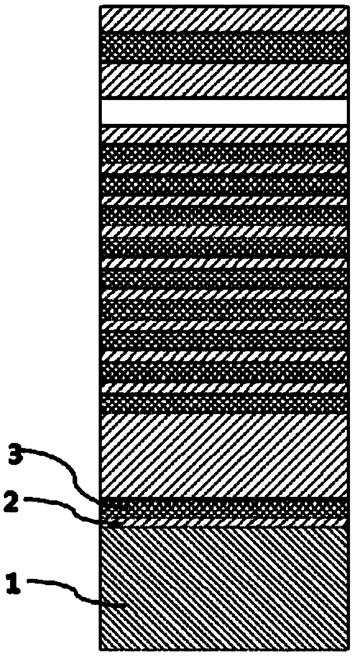
[0040] Please refer to Figure 1a-1m , the 3D NAND flash memory in the prior art adopts the following method:

[0041] S1: deposition substrate stack structure, see Figure 1a Specifically, a substrate 1 is provided, the surface of the substrate is formed with a multi-layer interlayer dielectric layer 2 and a sacrificial dielectric layer 3 interleaved, and the sacrificial dielectric layer 3 is formed between adjacent interlayer dielectric layers 2 ; The interlayer dielectric layer 2 is a silicon oxide layer, and the sacrificial dielectric layer 3 is a silicon nitride layer, thereby forming an O / N stack structure (O / N Stacks);

[0042] S2: ...


PUM


Abstract

The invention provides a 3D NAND manufacturing method and a memory. A back etching step of a sacrificial dielectric layer is added before each layer structure deposition step is performed on the channel hole of the 3D NAND structure, the etching area of the sacrificial dielectric layer in the channel hole region is increased, so that the opening area of the sacrificial dielectric layer is increased, and when each layer of structure in the channel, namely an ONOP structure, is formed through subsequent deposition, the ONOP laminated structure is located below the interlayer dielectric layer inthe plane of the sacrificial dielectric layer and plays a role in supporting the interlayer dielectric layer. The nitride layer in the O / N stack structure is subsequently removed and replaced with conductive metal, before a gate line is manufactured and formed, the ONOP structure located between the two adjacent interlayer dielectric layers in the channel hole plays a role in supporting the interlayer dielectric layers, so that the structures of the channel hole and the interlayer dielectric layers are more stable, and the risk that the interlayer dielectric layers are broken or collapsed after the sacrificial dielectric layer in the O / N stack structure is removed is reduced.

Description

technical field [0001] The invention relates to the technical field of semiconductor manufacturing, in particular to a 3D NAND manufacturing method and memory. Background technique [0002] With the development of planar flash memory, the production process of semiconductors has made great progress. However, in recent years, the development of planar flash memory has encountered various challenges: physical limits, existing development technology limits, and storage electron density limits. In this context, in order to solve the difficulties encountered in planar flash memory and to seek lower production costs per unit storage unit, various three-dimensional (3D) flash memory structures have emerged, such as 3D NOR (3D or not) flash memory and 3D NAND (3D NAND) flash memory. [0003] Wherein, in the 3D flash memory of the NOR structure, memory cells are arranged in parallel between the bit line and the ground line, while in the 3D flash memory of the NAND structure, the me...

Claims


Application Information

Patent Timeline
IPC IPC(8): H01L27/1157H01L27/11582H10B43/35H10B43/27
CPCH10B43/35H10B43/27
Inventor 杨永刚
Owner YANGTZE MEMORY TECH CO LTD
Features
  • R&D
  • Intellectual Property
  • Life Sciences
  • Materials
  • Tech Scout
  • Unparalleled Data Quality
  • Higher Quality Content
  • 60% Fewer Hallucinations
Learn More