Silicon wafer handover manipulator and silicon wafer handover device

A technology of manipulators and silicon wafers, which is applied in the field of lithography, can solve the problems affecting the exposure accuracy and yield of lithography machines, low efficiency of silicon wafer handover, and poor heat dissipation performance, so as to improve the efficiency of silicon wafer handover and heat dissipation performance, and improve Effect of Yield and Exposure Accuracy

Active Publication Date: 2020-02-21
SHANGHAI MICRO ELECTRONICS EQUIP (GRP) CO LTD
View PDF5 Cites 5 Cited by
  • Summary
  • Abstract
  • Description
  • Claims
  • Application Information

AI Technical Summary

Problems solved by technology

[0004] One object of the present invention is to propose a silicon wafer handover manipulator and a silicon wafer handover device to overcome the low efficiency of silicon wafer handover, low installation and debugging efficiency, and poor heat dissipation performance of the traditional silicon wafer handover device, which affect the exposure accuracy of the lithography machine. Yield Technical Issues

Method used


Image

  • Silicon wafer handover manipulator and silicon wafer handover device
  • Silicon wafer handover manipulator and silicon wafer handover device
  • Silicon wafer handover manipulator and silicon wafer handover device

Examples


Embodiment Construction

[0043] The technical solutions of the present invention will be further described below in conjunction with the accompanying drawings and through specific implementation methods.

[0044] In describing the present invention, it is to be understood that the terms "upper", "lower", "front", "rear", "left", "right", "vertical", "horizontal", "top", The orientation or positional relationship indicated by "bottom", "inner", "outer", etc. is based on the orientation or positional relationship shown in the drawings, and is only for the convenience of describing the present invention and simplifying the description, rather than indicating or implying the referred device Or elements must have a certain orientation, be constructed and operate in a certain orientation, and thus should not be construed as limiting the invention.

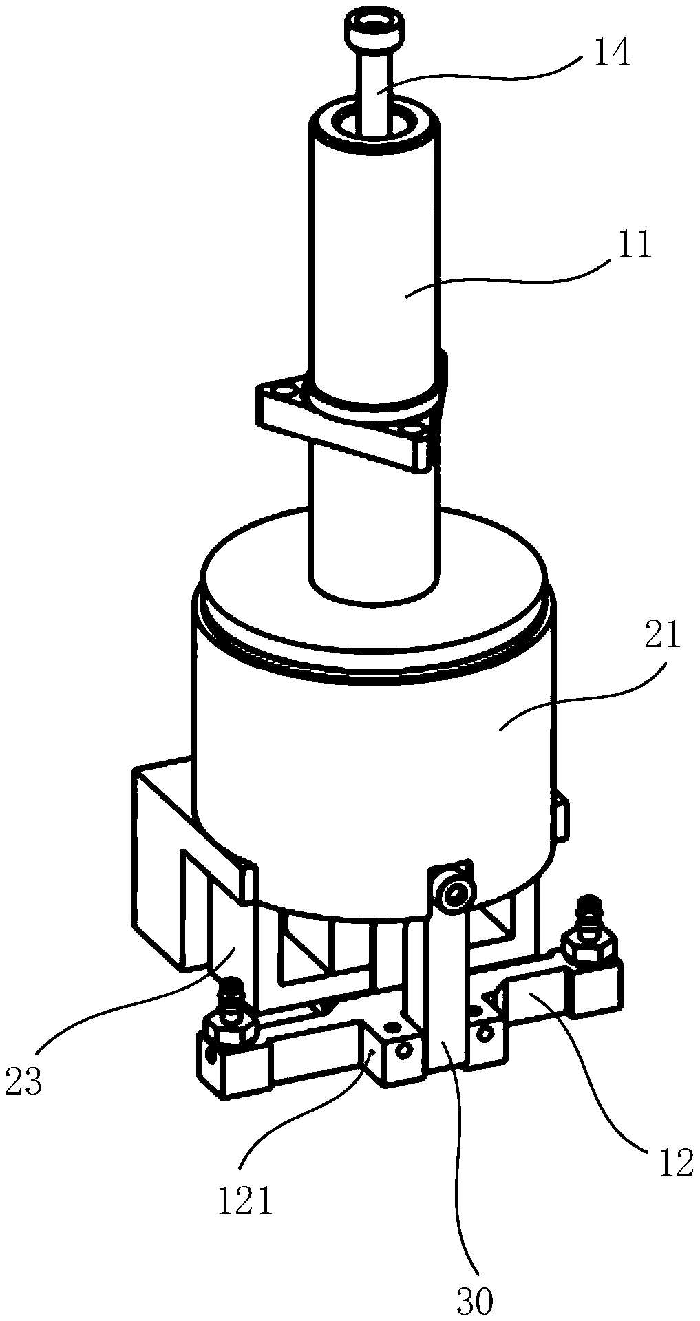
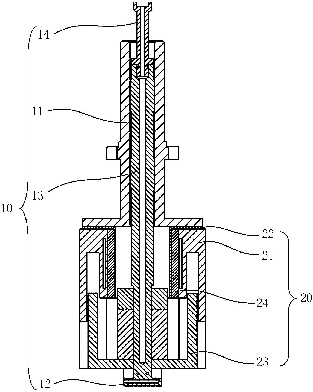
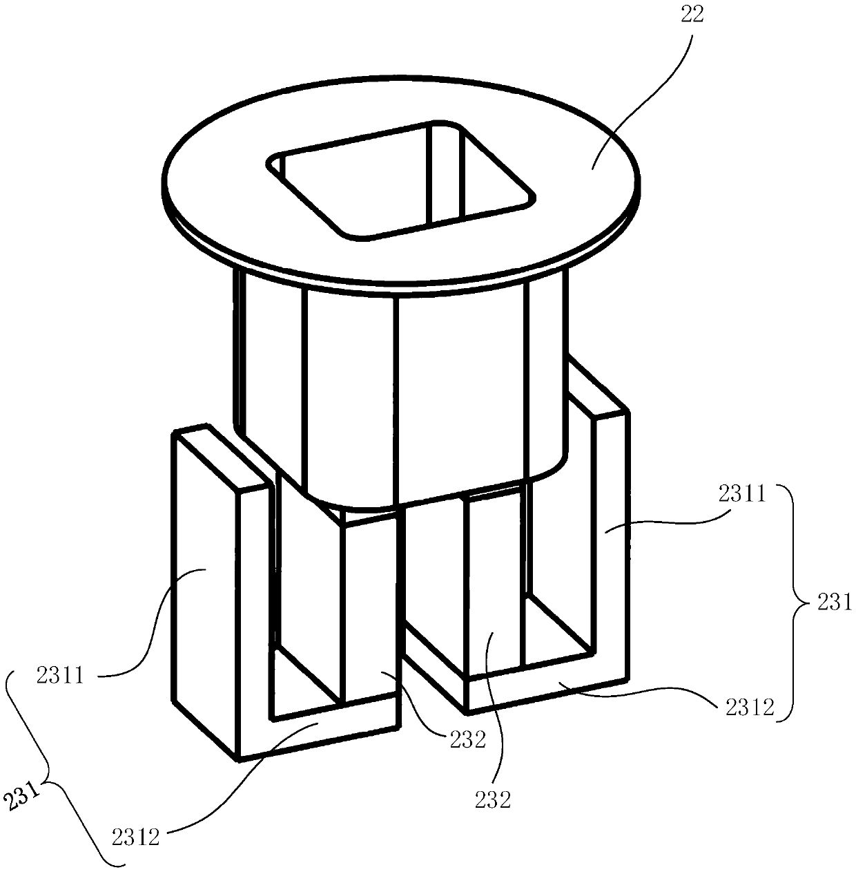
[0045] see Figures 1 to 4 In one embodiment, the silicon wafer handover manipulator includes an air flotation adsorption assembly 10 and a motor 20 driving th...


PUM

PropertyMeasurementUnit
thicknessaaaaaaaaaa

Abstract

The invention discloses a silicon wafer handover manipulator, a silicon wafer handover device and a photoetching machine. The silicon wafer handover manipulator comprises an air floatation adsorptionassembly and a motor; the motor comprises a base, a coil framework and two magnet assemblies; a coil is wound on the coil framework; the coil framework is connected with the inner side of the base ina sleeving manner; the two magnet assemblies are arranged under the coil framework in a spaced mode; each of the magnet assemblies is in a U shape; a U-shaped groove is opposite to the coil framework;the air floatation adsorption assembly comprises a shaft sleeve, a shaft seat, an air floatation shaft and an adsorption rod; the shaft sleeve is connected with the coil framework; the shaft seat isconnected with the two magnet assemblies; one end of the air floatation shaft is connected with the shaft seat; the other end of the air floatation shaft penetrates through a gap between the two magnet assemblies and the coil framework to extend into the shaft sleeve; and the adsorption rod is connected with the shaft sleeve in a sleeving manner and connected with the air floatation shaft. The silicon wafer handover manipulator can improve the yield and exposure precision of a photoetching machine. The invention further provides a silicon wafer handover device with the silicon wafer handover manipulator.

Description

technical field [0001] The invention relates to the field of photolithography technology, in particular to a silicon wafer handover manipulator and a silicon wafer handover device. Background technique [0002] In lithography equipment, the handover of silicon wafers requires a special handover manipulator to realize the functions of adsorption, linear transmission and release of silicon wafers. This series of actions needs to be completed quickly and maintain high reliability in a short period of time. With the improvement of the precision and productivity of lithography machines, the design of silicon wafer transfer devices is getting higher and higher. The traditional silicon wafer transfer devices using voice coil motors and mechanical guide rails can no longer meet the performance requirements. At present, the widely used high-precision silicon wafer handover device adopts voice coil motor and air bearing guide rail, and cooperates with grating ruler displacement measur...

Claims


Application Information

Patent Timeline
Patent Type & Authority Applications(China)
IPC IPC(8): G03F7/20B65G47/91B25J15/06
CPCB25J15/06B25J15/0616B25J15/0625B65G47/91G03F7/20
Inventor 刘屈武
Owner SHANGHAI MICRO ELECTRONICS EQUIP (GRP) CO LTD
Why Eureka
Try Eureka