

Composite conductive material
A technology of composite conductive and conductive material layers, which is applied in the direction of metal/alloy conductors, conductive layers on insulating carriers, oxide conductors, etc., can solve the problems of excessively wide display area borders, difficulty in minimizing the size of electronic devices, and cost increases. , to achieve the effect of reducing the overall resistance, improving reliability and reliability, and reducing the probability of occurrence
- Summary
- Abstract
- Description
- Claims
- Application Information
AI Technical Summary
Problems solved by technology
Method used
Image

Examples
Embodiment 1
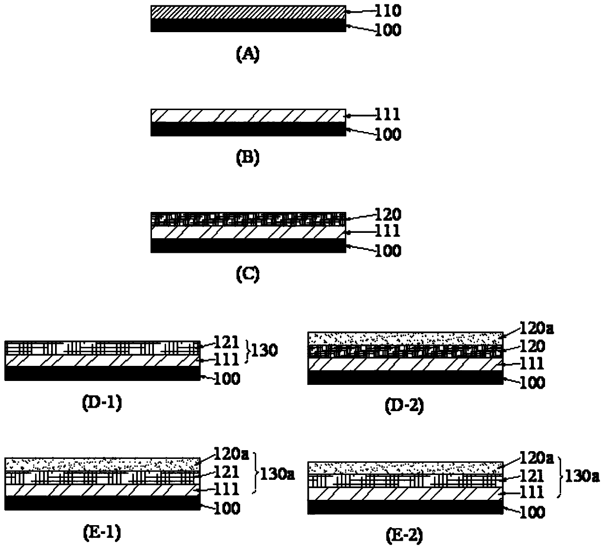
[0050] Such as figure 1 Shown is a schematic structural view of Embodiment 1 of the present invention.
[0051] Such as figure 1 As shown in (A), the ITO layer 110 is plated on the substrate 100 . Such as figure 1 As shown in (B), the ITO layer 110 is patterned into the ITO patterned layer 111 with a pattern 111p. Such as figure 1 Shown in (C), nano-silver wires are coated on the ITO patterned layer 111 to form a nano-silver wire layer 120, as figure 1 As shown in (D-1), the nano-silver wire layer 120 is patterned into a nano-patterned layer 121 , and the ITO patterned layer 111 is combined with the nano-patterned layer 121 to form a composite conductive material layer 130 . Such as figure 1 As shown in (E-1), after forming the composite conductive material layer 130, a layer of organic material 120a that is specially used to protect the nano-silver wire can be coated on the 130 composite conductive material layer, and the ITO patterned layer 111, the nano-pattern The c...
Embodiment 2
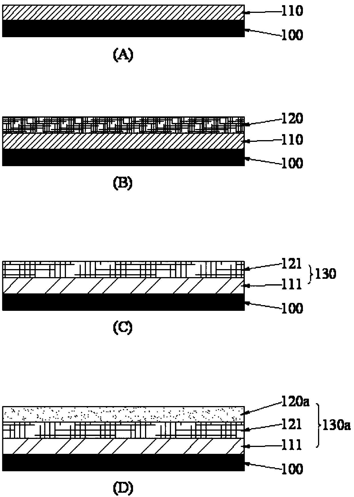
[0054] Such as figure 2 Shown is a schematic structural view of Embodiment 2 of the present invention. Embodiment 2 is similar to embodiment 1 and will not be repeated here.
[0055] Such as figure 2 As shown in (A), the ITO layer 110 is plated on the substrate 100 . Such as figure 2 As shown in (B), the nano-silver wire is coated on the ITO layer 110 to form the nano-silver wire layer 120 . Such as figure 2 As shown in (C), the ITO layer 110 and the nano-silver wire layer 120 are patterned simultaneously to obtain the ITO patterned layer 111 and the nano-patterned layer 121, and the conductive layer formed by combining the ITO patterned layer 111 and the nano-patterned layer 121 It is the composite conductive material layer 130 . Such as figure 2 As shown in (D), the organic material 120a can be coated on the composite conductive material layer 130, and the conductive layer formed by the ITO patterned layer 111, the nano-patterned layer 121 and the organic materia...
Embodiment 3
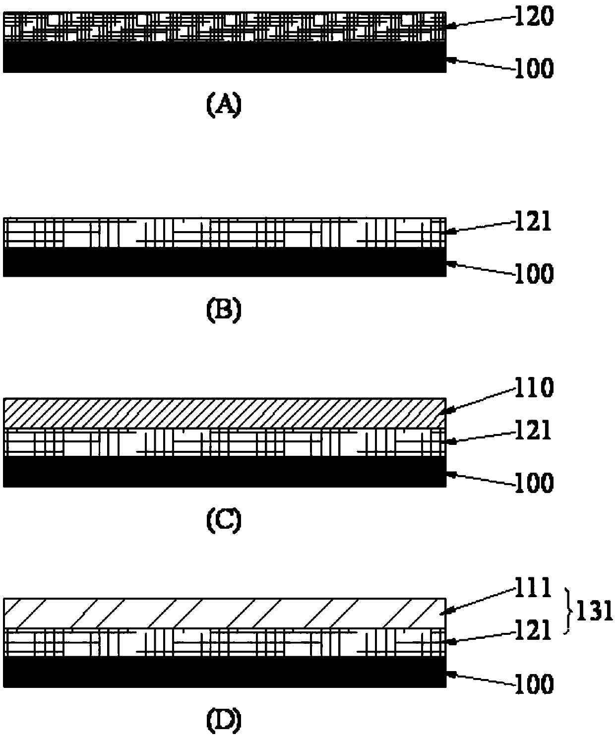
[0057] Such as image 3 Shown is a schematic structural view of Embodiment 3 of the present invention. Embodiment 3 is similar to Embodiment 1 and will not be repeated here.
[0058] Such as image 3 As shown in (A), the nano silver wire layer 120 is coated on the substrate 100 . Such as image 3 As shown in (B), the nano-silver wire layer 120 is patterned into a nano-patterned layer 121 . Such as image 3 As shown in (C), the nano-patterned layer 121 is plated with the ITO layer 110 . Such as image 3 As shown in (D), the ITO layer 110 is patterned into an ITO patterned layer 111 , and the conductive layer formed by the nano-patterned layer 121 and the ITO patterned layer 111 is a composite conductive material layer 131 .
PUM
 Abstract
Description
Claims
Application Information