Quasi-optical system for terahertz beam shaping

A beam shaping and optical system technology, applied in the field of quasi-optical systems, can solve the problems of poor lens matching, signal attenuation, low transmittance, etc., and achieve the effects of improving system resolution, controlling chromatic aberration, and reducing absorption

Pending Publication Date: 2020-03-17
青岛青源峰达太赫兹科技有限公司
View PDF0 Cites 2 Cited by
  • Summary
  • Abstract
  • Description
  • Claims
  • Application Information

AI Technical Summary

Problems solved by technology

It overcomes the shortcomings of the current common terahertz beam transmission optical path lens,

Method used


Image

  • Quasi-optical system for terahertz beam shaping
  • Quasi-optical system for terahertz beam shaping
  • Quasi-optical system for terahertz beam shaping

Examples


Embodiment 1

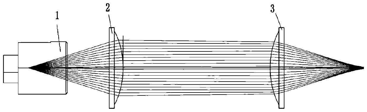
[0026] The quasi-optical system used for terahertz beam shaping involved in this embodiment includes a flat semiconductor crystal 1, a hyper-hemispherical silicon lens 2, and a collimator lens 3. One side of the hyper-hemispherical silicon lens 2 is a hyper-hemispherical surface, and the other side is a plane. The flat semiconductor The crystal 1 is glued to the plane side of the super hemispherical silicon lens 2, the collimator lens 3 is placed on the hyper hemispherical side of the hyper hemispherical silicon lens 2, and the optical axes of the flat semiconductor crystal 1, the hyper hemispherical silicon lens 2 and the collimation lens 3 coincide. The super hemispherical silicon lens 2 adopts high-resistance silicon material. The refractive index of semiconductor crystal material is generally 3.4-3.6, and the critical angle of total reflection in air is 16.13°-17.10°. High-resistance silicon with a refractive index similar to that of semiconductor crystal material is used A...

Embodiment 2

[0034] The quasi-optical system used for terahertz beam shaping involved in this embodiment includes a flat semiconductor crystal 1, a hyper-hemispherical silicon lens 2, a collimator lens 3, a focusing lens 4 and a focal plane 5, and one side of the hyper-hemispherical silicon lens 2 is a hyper-hemispheric One side is a plane, the flat semiconductor crystal 1 is glued to the plane side of the super hemispherical silicon lens 2, the collimating lens 3 is placed on the super hemispherical side of the hyper hemispherical silicon lens 2, and the focusing lens 4 is placed on the side of the collimating lens 3, The collimating lens 3 is close to the convex surface of the focusing lens 4, the focal plane 5 is placed at the focal point of the focusing lens 4, and the optical axes of the flat semiconductor crystal 1, the super hemispherical silicon lens 2, the collimating lens 3 and the focusing lens 4 coincide.

[0035] Further, the super hemispherical surface of the super hemispherical...


PUM

PropertyMeasurementUnit
Diameteraaaaaaaaaa

Abstract

The invention discloses a quasi-optical system for terahertz beam shaping. The system comprises a flat semiconductor crystal, a super-hemispherical silicon lens and an aspheric collimating lens, wherein one surface of the super-hemisphere silicon lens is a super-hemisphere surface, and the other surface of the super-hemisphere silicon lens is a plane; the flat semiconductor crystal is fixed on theplane side of the super-hemisphere silicon lens; and the aspheric collimating lens is arranged on the super-hemisphere side of the super-hemisphere silicon lens. The flat semiconductor crystal generates collimated terahertz waves under the excitation of femtosecond laser pulses and direct-current bias voltage; and the generated terahertz waves directly enter the super-hemispherical silicon lens and the aspheric collimating lens, and parallel terahertz wave beams are output. The system can also comprise an aspheric focusing lens and a focal plane; and the parallel terahertz wave beams enter the aspheric focusing lens and reach the position of the test focal plane to generate focused terahertz waves. The influence of water vapor absorption is reduced, the system resolution is improved, theproportion of total reflection beams is reduced, the maximum transmittance reaches 72%, meanwhile, the optical path of an air optical path is reduced, and the terahertz signal quality is improved.

Description

Technical field: [0001] The invention belongs to the technical field of terahertz spectroscopy and imaging technology, and in particular relates to a quasi-optical system for terahertz beam shaping. Background technique: [0002] Terahertz refers to an electromagnetic wave with a frequency between 0.1THz-10THz, which is located between infrared and millimeter waves on the spectrum. The research on terahertz has been in a blank stage for a long time. Since the 1980s, with the development of ultrafast With the development of optoelectronic technology and low-scale semiconductor technology, people have gradually begun to study the terahertz band. As an emerging technology, terahertz technology has been valued by governments of various countries. In 2004, it was rated as one of the "Ten Technologies that Will Change the Future World" by the United States. The Xiangshan Science Conference with the theme of terahertz was also held. [0003] Terahertz wave has many unique advanta...

Claims


Application Information

Patent Timeline
IPC IPC(8): G02B27/09
CPCG02B27/0955
Inventor 朱新勇王玉建刘永利张朝惠
Owner 青岛青源峰达太赫兹科技有限公司
Why Eureka
Try Eureka