Wafer polishing device and method

A technology for polishing devices and wafers, which is applied in the direction of grinding devices, electrical components, circuits, etc., which can solve the problems of shortened service life of polishing carriers, decreased flatness of wafers, and increased costs, so as to improve flatness and prolong use The effect of life, polishing process is simple and easy

Inactive Publication Date: 2020-03-24
SHANGHAI ADVANCED SILICON TECH CO LTD +1
View PDF9 Cites 3 Cited by
  • Summary
  • Abstract
  • Description
  • Claims
  • Application Information

AI Technical Summary

Problems solved by technology

In the current polishing process technology, wafers of different thicknesses need to use polishing carriers with different groove depths.

Method used


Image

  • Wafer polishing device and method
  • Wafer polishing device and method
  • Wafer polishing device and method

Examples


Embodiment 1

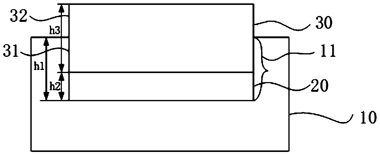
[0031] figure 1 A schematic structural diagram of a wafer polishing device provided in Embodiment 1 of the present invention, as shown in figure 1 As shown, the wafer polishing device includes a polishing carrier 10 and an adjustable thickness polishing pad 20. The polishing carrier 10 includes a polishing carrier groove 11. During the polishing process of the wafer 30, the thickness adjustable polishing pad 20 is arranged on In the polishing carrier slot 11 , the wafer 30 is placed on the polishing pad 20 with adjustable thickness.

[0032] The groove depth h1 of the polishing carrier groove 11 , the thickness h2 of the thickness-adjustable polishing pad, and the thickness h3 of the wafer satisfy h2+h3>h1.

[0033] It should be noted that the thickness-adjustable polishing pad 20 is selected according to the thickness h3 of the wafer 30 . When the sum of the thickness h2 of the thickness-adjustable polishing pad and the thickness h3 of the wafer is greater than the groove d...

Embodiment 2

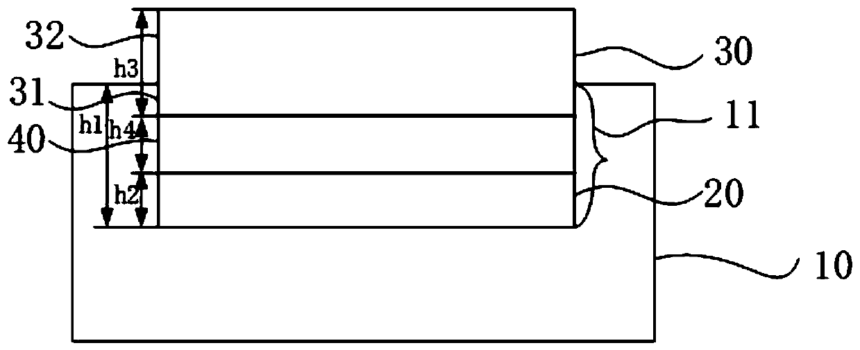
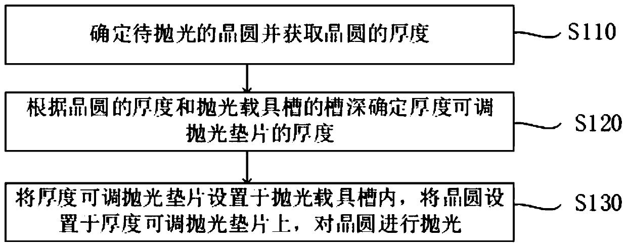
[0055] image 3 It is a schematic flow chart of a wafer polishing method provided in Embodiment 2 of the present invention. A wafer 30 is polished using a wafer polishing device. Refer to Figure 1-3 , the wafer polishing device includes a polishing carrier 10 and a thickness-adjustable polishing pad 20, the polishing carrier 10 includes a polishing carrier groove 11, and the wafer polishing method includes:

[0056] S110. Determine the wafer to be polished and acquire the thickness of the wafer.

[0057] S120. Determine the thickness of the polishing pad with adjustable thickness according to the thickness of the wafer and the groove depth of the polishing carrier groove.

[0058] Wherein, the groove depth h1 of the polishing carrier groove 11 , the thickness h2 of the adjustable thickness polishing pad 20 and the thickness h3 of the wafer 30 satisfy h2+h3>h1.

[0059] S130 disposing the thickness-adjustable polishing pad in the groove of the polishing carrier, setting the ...


PUM

PropertyMeasurementUnit
Thicknessaaaaaaaaaa
Thicknessaaaaaaaaaa

Abstract

The invention discloses a wafer polishing device and method. The wafer polishing device comprises a polishing carrier and a thickness-adjustable polishing gasket, the polishing carrier comprises a polishing carrier groove, in the wafer polishing process, the thickness-adjustable polishing gasket is arranged in the polishing carrier groove, and a wafer is arranged on the thickness-adjustable polishing gasket; the groove depth h1 of the polishing carrier groove, the thickness h2 of the thickness-adjustable polishing gasket and the thickness h3 of the wafer meet the formula that h2+h3>h1. The wafer polishing device has the advantages that the service life of the wafer polishing device is prolonged, the flatness of the wafer can be improved, and the polishing process is simple and easy to implement.

Description

technical field [0001] Embodiments of the present invention relate to the technical field of semiconductor manufacturing, and in particular, to a wafer polishing device and method. Background technique [0002] The semiconductor industry is the core of the modern electronics industry. At present, more than 90% of semiconductor devices and circuits, especially Ultra Large Scale Integrated circuits (ULSI), are manufactured on high-purity and high-quality single crystal polished wafers and epitaxial wafers. . Therefore, it is particularly important to obtain wafers with extremely small surface micro-defects and high flatness in the wafer manufacturing process. [0003] The polishing process is a process required to process the wafer to a specified thickness and improve the flatness of the wafer, and is performed using a polishing device that polishes the wafer. In the current polishing process technology, wafers of different thicknesses need to use polishing carriers with dif...

Claims


Application Information

Patent Timeline
IPC IPC(8): B24B37/10B24B37/20B24B37/30H01L21/304
CPCB24B37/107B24B37/20B24B37/30H01L21/304
Inventor 张黎欢沈思情孙强张俊宝陈猛
Owner SHANGHAI ADVANCED SILICON TECH CO LTD
Why Eureka
Try Eureka