Surface acoustic wave module one-step molded packaging structure and packaging process thereof

A surface acoustic wave and packaging structure technology, applied in electrical components, impedance networks, etc., can solve the problems of affecting performance, affecting shielding effect, single chip function, etc., and achieve the effect of reducing the package size, good shielding effect, and good overall performance.

Pending Publication Date: 2020-04-17
天通瑞宏科技有限公司
View PDF0 Cites 6 Cited by
  • Summary
  • Abstract
  • Description
  • Claims
  • Application Information

AI Technical Summary

Problems solved by technology

[0002] At present, surface acoustic wave filters have high requirements on the cleanliness of the working surface. Usually, the bare chip is packaged separately, but the function of a single chip is single, which cannot meet the requirements of high integration of modern electronic products, and often needs to be combined with other functional devices. Perform secondary packaging, but this increases the volume of the integrated module, which is contrary to the concept of miniaturization
At the same time, the shielding of the surface acoustic filter is very important to its performance. If there is signal interference, it will have a great impact on the filtering effect. The current packaging is injection molded, and then nickel-plated to achieve shielding. The metal shielding layer is located on the device. The outermost layer, in the subsequent assembly process, may damage the metal layer, thereby affecting the shielding effect
And it can only satisfy the isolation inside and outside the module. In fact, due to the high integration of the module, the number and functions of the components inside the module are increasing, and they will also interfere with each other, affecting performance.

Method used


Image

  • Surface acoustic wave module one-step molded packaging structure and packaging process thereof
  • Surface acoustic wave module one-step molded packaging structure and packaging process thereof
  • Surface acoustic wave module one-step molded packaging structure and packaging process thereof

Examples


Embodiment 1

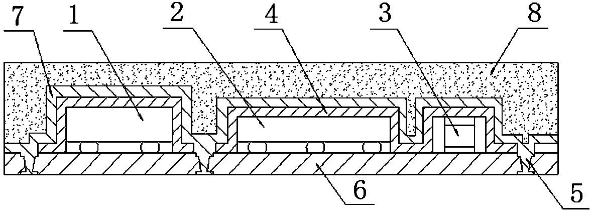
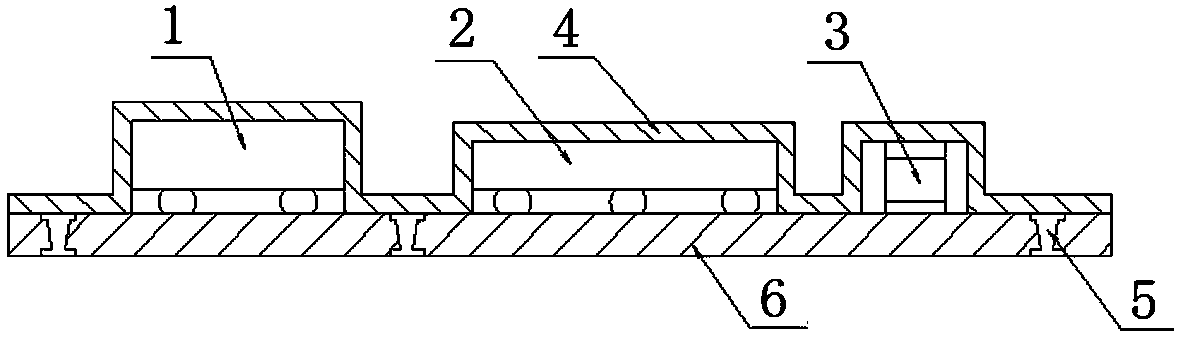
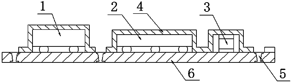
[0023] Embodiment 1: as attached figure 1 As shown, a packaging structure of a surface acoustic wave module is formed at one time, including a laminated board 6, and five acoustic surface bare chips 1, active devices 2 and passive devices 3 are arranged on the laminated board 6, and the active device 2 The device 2 includes a switch and an LNA. The passive device 3 includes three capacitors and four inductors. The laminated board 6 is provided with a via hole connection ground PAD5. An epoxy resin film 4 is provided on the mounting surface of the device 2 and the passive device 3, and a nickel layer 7 is provided on the epoxy resin film 4, and the nickel layer 7 is connected to the ground pad on the front side and the pad on the back side through a via hole. The ground PAD5 encapsulates the EMC layer 8 on the periphery of the nickel layer 7, and the EMC layer 8 is epoxy resin molding compound.

Embodiment 2

[0024] Embodiment 2: A packaging process for a packaging structure of a surface acoustic wave module, comprising the following steps,

[0025] In the first step, the SAW bare chip 1, the active device 2 and the passive device 3 are mounted on the laminate 6 through the SMT patch, gold ball flip chip or solder ball flip chip process; the active device 2 includes a A switch and an LNA, the passive device 3 includes three capacitors and four inductors;

[0026] In the second step, cover the epoxy resin film 4 on the mounting surface of the acoustic surface bare chip 1, active device 2 and passive device 3, and after lamination by vacuum lamination equipment, solidify in an oven (such as figure 2 shown); the film has a good combination with the laminate and the device, and there is no resin filling at the bottom of the device, which can ensure the normal function of the surface acoustic wave device;

[0027] The third step is to pass the laminated plate of the cured epoxy resin ...

Embodiment 3

[0030] Embodiment 3: The packaging structure of the second surface acoustic wave module at one time, including a laminate 6, on which four SAW bare chips 1 and active devices 2 are arranged, and the active device 2 Includes a switch. The metal plating layer 7 is a copper layer. Others are the same as in Example 1.


PUM


Abstract

The invention discloses a surface acoustic wave module one-time formed packaging structure and a packaging process thereof. According to the packaging structure, a surface acoustic wave bare chip, anactive device and a passive device are arranged on a laminated board, and a via hole is formed in the laminated board to be connected with a ground PAD; a thin film and a metal coating are sequentially arranged on the mounting surface of each device, wherein the metal coating is connected with the ground pad on the front face and the ground PAD on the back face through via holes, and an EMC layeris packaged on the periphery of the metal coating. The packaging process comprises the following steps: mounting each device on the laminated board; covering the mounting surface of each device with the thin film for curing; then removing the thin film on the surface of the grounding PAD through laser equipment, and setting a metal plating layer to enable the metal plating layer to be conducted with the grounding PAD; and finally filling the EMC layer. According to the invention, the shielding area can be flexibly created, the packaging size is reduced, and the heat dissipation is better through the shielding layer; and compared with the traditional process, the process enables the metal shielding layer to be protected inside, so the reliability is better, the shielding effect is good, andthe overall performance is better.

Description

technical field [0001] The invention relates to a package structure of a filter and a package process thereof, in particular to a package structure of a surface acoustic wave module formed at one time and a package process thereof. Background technique [0002] At present, surface acoustic wave filters have high requirements on the cleanliness of the working surface. Usually, the bare chip is packaged separately, but the function of a single chip is single, which cannot meet the requirements of high integration of modern electronic products, and often needs to be combined with other functional devices. Perform secondary packaging, but this increases the volume of the integrated module, which is contrary to the concept of miniaturization. At the same time, the shielding of the surface acoustic filter is very important to its performance. If there is signal interference, it will have a great impact on the filtering effect. The current packaging is injection molded, and then ni...

Claims


Application Information

Patent Timeline
Patent Type & Authority Applications(China)
IPC IPC(8): H03H9/64
CPCH03H9/64
Inventor 王婕朱德进綦超张伟刘石桂
Owner 天通瑞宏科技有限公司
Why Eureka
Try Eureka