Agglomerating nanoparticles
A technology of nanoparticles and particles, which is applied in the field of agglomerating nanoparticles to form larger aggregates, which can solve problems such as false triggering and abnormal changes in device pressure sensitivity
- Summary
- Abstract
- Description
- Claims
- Application Information
AI Technical Summary
Problems solved by technology
Method used
Image
Examples
Embodiment 1
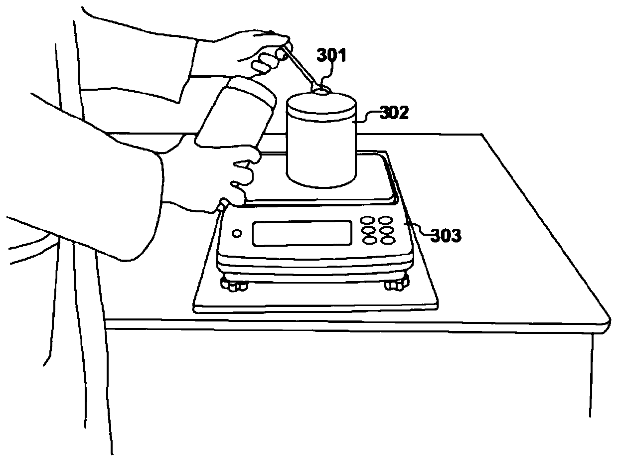
[0068] • A millbase was formulated with a formulation of 900 grams (900g) of VA401 resin and 28 grams (28g) of FS10P particles.
[0069] • The formulation was mixed in a high speed mixer at 1600 revolutions per minute (1600 rpm) to produce a first mixture.
[0070] • Bead mill at a power of 750 watts (750W) to produce a second mixture.
[0071] • High speed mixing again at 1600 revolutions per minute (1600 rpm).
[0072] • The second mixture was filtered through a 10 micron (10 μm) stainless steel filter to obtain a millbase.
[0073] Thus, in this example, the prepared millbase contained 3% by weight (3 wt%) nanoparticles of the resin. In this way, the prepared millbase exhibited a higher loading of resin compared to conventional methods.
[0074] Figure 12
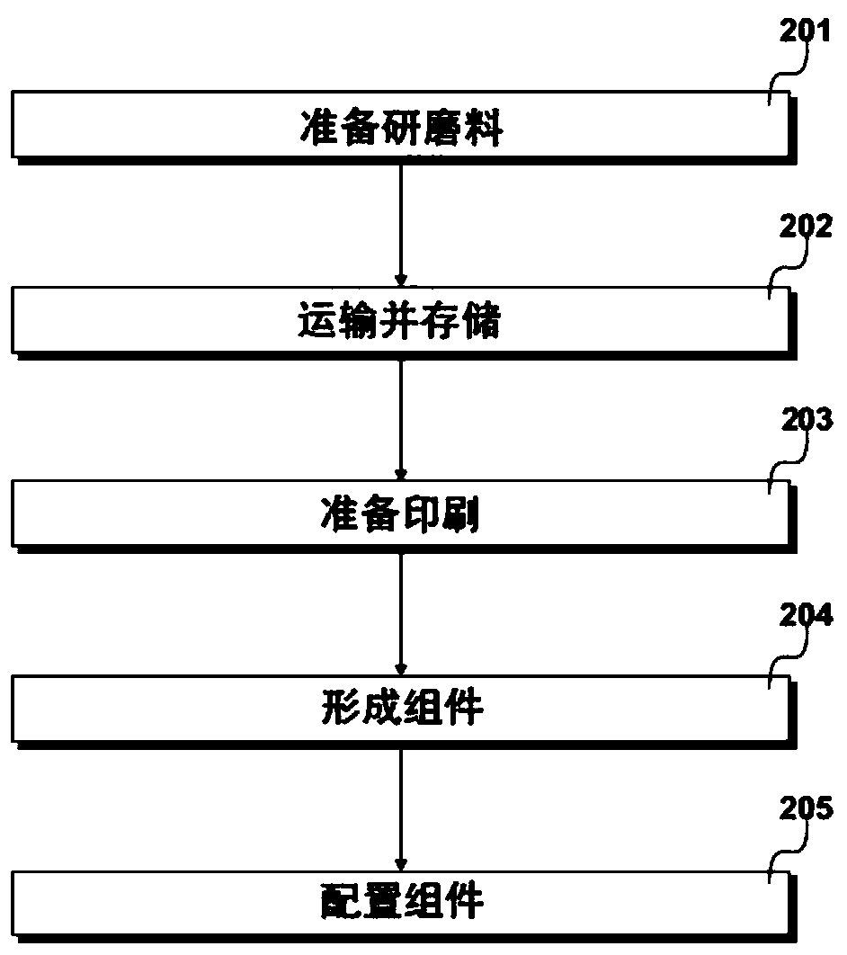
[0075] Figure 12 The process 203 for cutting the abrasive 109 to obtain a formulated mixture ready for printing is described in detail in . The stored grind 1009 is now cut by solvent 1201 to obtain a formulated...
Embodiment 2
[0078] • To obtain the formulated mixture, the filtered grind was mixed at high speed at 1600 revolutions per minute (1600 rpm) for one minute.
[0079] • Pour 25 grams (25g) of the grind into the container.
[0080] • Add 15 grams (15 g) of solvent ZV558 followed by 11.7 grams (11.7 g) of VA401 lacquer.
[0081] • Mix at high speed for 1 minute (1 min) at 3500 revolutions per minute (3500 rpm).
[0082] • Add 19 milligrams (19 mg) of dielectric particles under the tradename Aston Chemicals MST-547.
[0083] - Further high speed mixing at 3500 revolutions per minute (3500 rpm) for 1 minute (1 min).
[0084] After conditioning, it was found that the printed sensor did not suffer from any electrical short circuit failures. Thus, a more consistent electrical response is obtained. Furthermore, the material exhibits higher transparency and exhibits lower haze.
[0085] Figure 13
[0086] Figure 13 to Figure 15 A process 204 for forming a component is described. For deplo...
PUM
| Property | Measurement | Unit |
|---|---|---|
| size | aaaaa | aaaaa |
| size | aaaaa | aaaaa |
| size | aaaaa | aaaaa |
Abstract
Description
Claims
Application Information


