Duplexer
A duplexer and resonator technology, which is applied in the field of high power capacity duplexers, can solve problems such as degraded device performance, and achieve the effects of optimizing device performance, reducing device thermal resistance, and reducing inductive coupling
- Summary
- Abstract
- Description
- Claims
- Application Information
AI Technical Summary
Problems solved by technology
Method used
Image

Examples
Embodiment 1
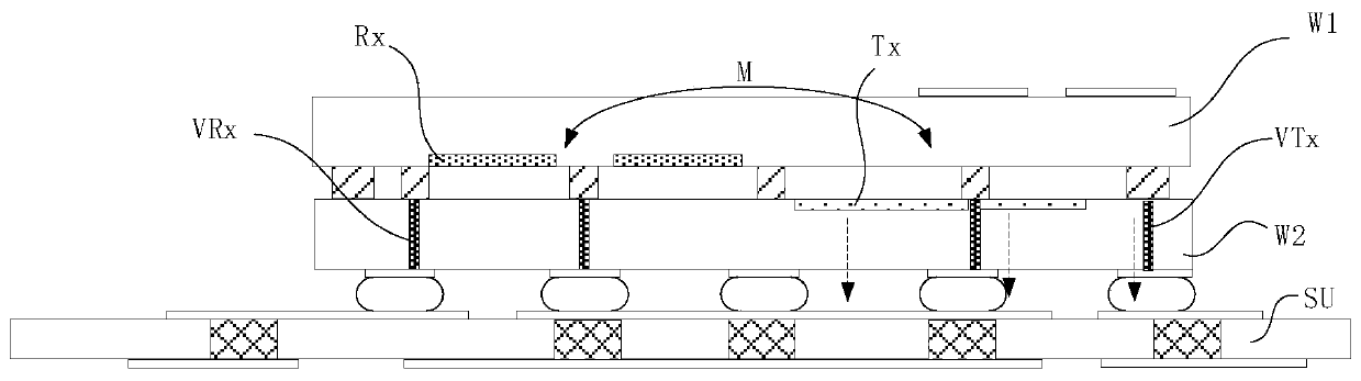
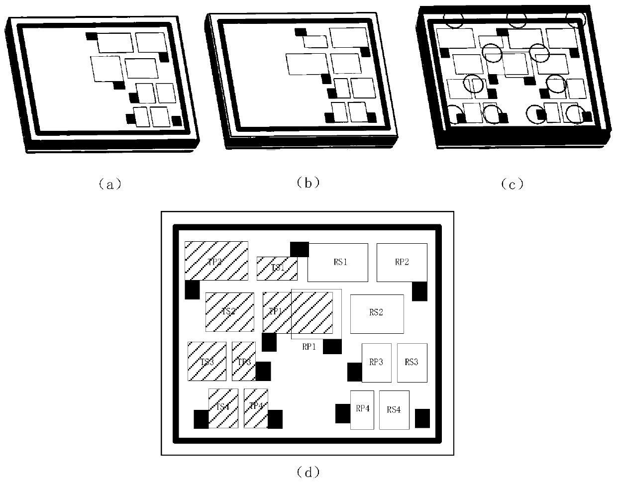
[0036] figure 2 is a schematic cross-sectional view of a duplexer 100 according to an embodiment of the present invention. image 3 It is a schematic diagram of the assembly of the duplexer, specifically: (a) is a front schematic diagram of a wafer assembly with a transmit filter Tx; (b) is a front schematic diagram of a wafer assembly with a receive filter Rx; (c) is Front schematic diagram of duplexer chip assembly; (d) is a perspective view of the duplexer chip viewed from the side of the wafer where the transmit filter Tx is located. Figure 4 is the circuit diagram of the duplexer.
[0037] Such as figure 2 with image 3 It can be seen that, from the perspective of device structure, the duplexer 100 has a packaging substrate SU, an upper wafer W1 on which a transmitting filter Tx is fabricated, and a lower wafer W2 on which a receiving filter Rx is fabricated. The upper wafer W1 is packaged with the lower wafer W2 through wafer bonding, and then connected to the top...
Embodiment 2
[0044] Figure 7 is a schematic cross-sectional view of a duplexer 200 according to Embodiment 2 of the present invention. Figure 8 It is a circuit diagram of the duplexer 200 in the second embodiment of the present invention.
[0045] From the perspective of device structure, compared with the duplexer 100, the duplexer 200 also includes an isolation wafer W3. The isolated wafer W3 is arranged between the upper wafer W1 and the lower wafer W2, the upper surface of the isolated wafer W3 is bonded to the lower surface of the upper wafer W1 and the lower surface of the isolated wafer W3 is bonded to the lower surface of the lower wafer W2. bonded to the top surface. The material of the isolation wafer W3 may be a silicon wafer, which has the advantage of being universal and easy to obtain. The thickness of the isolation wafer W3 is generally 30 to 150 microns. Adding the isolation wafer W3 can increase the distance between the upper wafer W1 and the lower wafer W2 from the ...
Embodiment 3
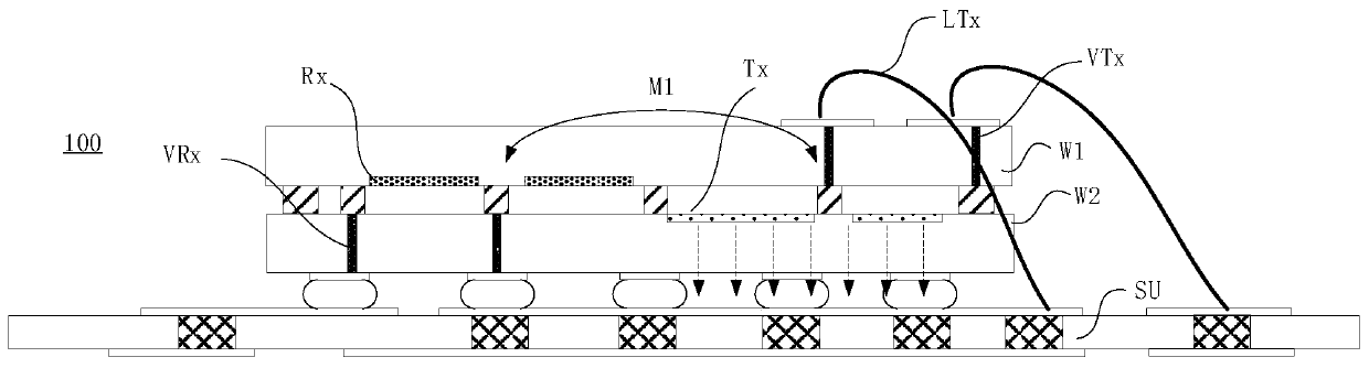
[0049] Figure 10 is a schematic cross-sectional view of a triple duplexer 300 according to an embodiment of the present invention.
[0050] Such as Figure 10 As shown, the duplexer is formed by two wafers bonded and packaged, including a package substrate SU, a receive filter Rx located in the upper wafer W1 and a transmit filter Tx located in the lower wafer W2.
[0051] In the receiving filter Rx, the receiving resonator that needs to be connected to the outside is connected to the pad on the upper surface of the upper wafer through the via hole VRx made on the upper wafer, and then connected to the package substrate SU through the bonding wire LRx The bonding fingers on the top are connected. In the transmit filter Tx, the transmit resonator that needs to be connected to the outside is connected to the pad on the lower surface of the lower wafer W2 through the via hole VTx made on the lower wafer W2, and then through the solder ball and the package carrier below SU con...
PUM
| Property | Measurement | Unit |
|---|---|---|
| thickness | aaaaa | aaaaa |
Abstract
Description
Claims
Application Information
 - R&D
- Intellectual Property
- Life Sciences
- Materials
- Tech Scout
- Unparalleled Data Quality
- Higher Quality Content
- 60% Fewer Hallucinations
Browse by: Latest US Patents, China's latest patents, Technical Efficacy Thesaurus, Application Domain, Technology Topic, Popular Technical Reports.
© 2025 PatSnap. All rights reserved.Legal|Privacy policy|Modern Slavery Act Transparency Statement|Sitemap|About US| Contact US: help@patsnap.com