Supercharge Your Innovation With Domain-Expert AI Agents!

An optoelectronic semiconductor processing system

A technology of optoelectronic semiconductors and processing systems, applied in the field of optoelectronics, can solve the problems of machine damage, cumbersome handling process, bulky volume, etc., and achieve the effect of convenient processing and convenient lateral movement

Active Publication Date: 2021-10-22
ZHENGZHOU UNIVERSITY OF LIGHT INDUSTRY
View PDF6 Cites 0 Cited by
  • Summary
  • Abstract
  • Description
  • Claims
  • Application Information

AI Technical Summary

Problems solved by technology

[0003] Aiming at the deficiencies of the prior art, the present invention provides an optoelectronic semiconductor processing system, which solves the problem that the existing semiconductor cutting device is very cumbersome in the handling process due to its bulky volume and is easy to machine problem causing damage

Method used


Image

  • An optoelectronic semiconductor processing system
  • An optoelectronic semiconductor processing system
  • An optoelectronic semiconductor processing system

Examples


Embodiment Construction

[0028] The following will clearly and completely describe the technical solutions in the embodiments of the present invention with reference to the accompanying drawings in the embodiments of the present invention. Obviously, the described embodiments are only some of the embodiments of the present invention, not all of them. Based on the embodiments of the present invention, all other embodiments obtained by persons of ordinary skill in the art without making creative efforts belong to the protection scope of the present invention.

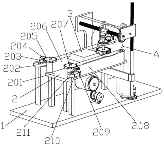
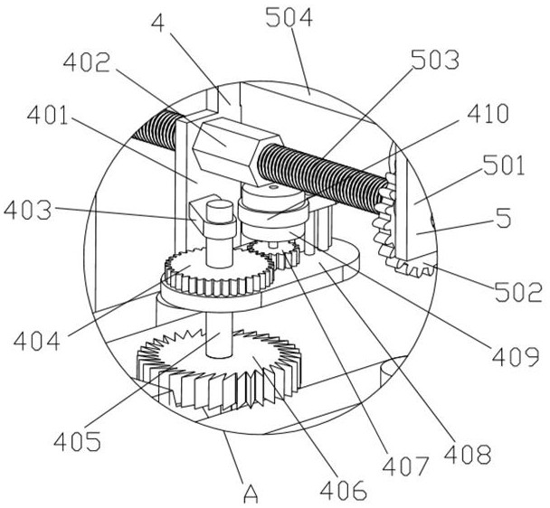
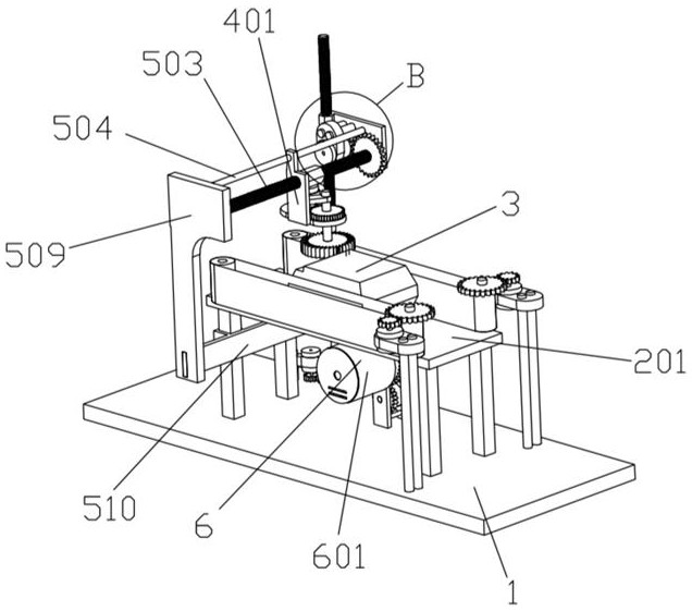
[0029] see figure 1 , figure 2 , image 3 , Figure 4 , Figure 5 , Figure 6 , Figure 7 An optoelectronic semiconductor processing system shown includes a supporting base 1, a clamping and conveying module 2, a silicon shell 3, a cutting module 4, a lateral displacement system 5, a suction cup module 6, a supporting column 7 and a longitudinal driving module 8, and the supporting base 1 The clamping and conveying module 2 is fixedly conn...


PUM


Abstract

The invention discloses a photoelectric semiconductor processing system, which includes a support base, a clamping and conveying module, a silicon shell, a cutting module, a lateral displacement system, a sucker module, a support column and a longitudinal drive module, and the upper part of the support base is fixedly connected with a support column. Clamping the conveying module, the middle part of the clamping conveying module is overlapped with a silicon shell, a cutting module is arranged above the silicon shell, and a lateral displacement system is arranged on the top of the cutting module. The present invention can move the silicon shell to the corresponding position through the clamping and conveying module, and can clamp the silicon shell through the friction between the right conveyor belt and the left conveyor belt and the silicon shell, and through the set cutting module, It can drive the cutting wheel to rotate to facilitate the processing of the silicon shell, so as to correct the shape of the silicon shell. By setting the lateral displacement system, the lateral movement of the cutting module is facilitated, so as to realize the horizontal processing of the silicon shell. By setting the suction cup module, it is convenient to move the The silicon shell is attracted to the upper surface of the transport chassis.

Description

technical field [0001] The invention relates to the technical field of optoelectronics, in particular to an optoelectronic semiconductor processing system. Background technique [0002] A semiconductor refers to a material whose conductivity at room temperature is between that of a conductor and an insulator. Semiconductors are used in integrated circuits, consumer electronics, communication systems, photovoltaic power generation, lighting applications, high-power power conversion and other fields. For example, a diode is a device made of a semiconductor. No matter from the perspective of technology or economic development, the importance of semiconductors is huge. The core units of most of today's electronic products, such as computers, mobile phones or digital recorders, are closely related to semiconductors. Common semiconductor materials include silicon, germanium, gallium arsenide, etc., and silicon is the most influential one in commercial applications among various...

Claims


Application Information

Patent Timeline
Patent Type & Authority Patents(China)
IPC IPC(8): B28D5/02B28D7/04B28D7/00
CPCB28D5/0058B28D5/0094B28D5/022
Inventor 张雪龄金听祥程传晓赵汉章王志伟
Owner ZHENGZHOU UNIVERSITY OF LIGHT INDUSTRY
Features
  • R&D
  • Intellectual Property
  • Life Sciences
  • Materials
  • Tech Scout
  • Unparalleled Data Quality
  • Higher Quality Content
  • 60% Fewer Hallucinations
Learn More