Method and system for manufacturing modulation-free array structure by adopting laser interference photoetching technology

A laser interference lithography and array structure technology, which is applied in the field of laser interference lithography to produce non-modulated array structures, can solve the problems of not being too harsh in use conditions, and achieve the effects of low production difficulty, good stability, and high production efficiency

Inactive Publication Date: 2020-04-28
CHANGCHUN INST OF OPTICS FINE MECHANICS & PHYSICS CHINESE ACAD OF SCI
View PDF6 Cites 2 Cited by
  • Summary
  • Abstract
  • Description
  • Claims
  • Application Information

AI Technical Summary

Problems solved by technology

[0006] Aiming at the phenomenon of modulation in existing laser interference lithography patterns, the embodiment of the present invention provides a method and method for a non-modulation array structure using laser interference lithography technology that is suitable for mass production, the use conditions are not too harsh, and non-modulation periodicity is generated. system

Method used


Image

  • Method and system for manufacturing modulation-free array structure by adopting laser interference photoetching technology
  • Method and system for manufacturing modulation-free array structure by adopting laser interference photoetching technology
  • Method and system for manufacturing modulation-free array structure by adopting laser interference photoetching technology

Examples


Embodiment Construction

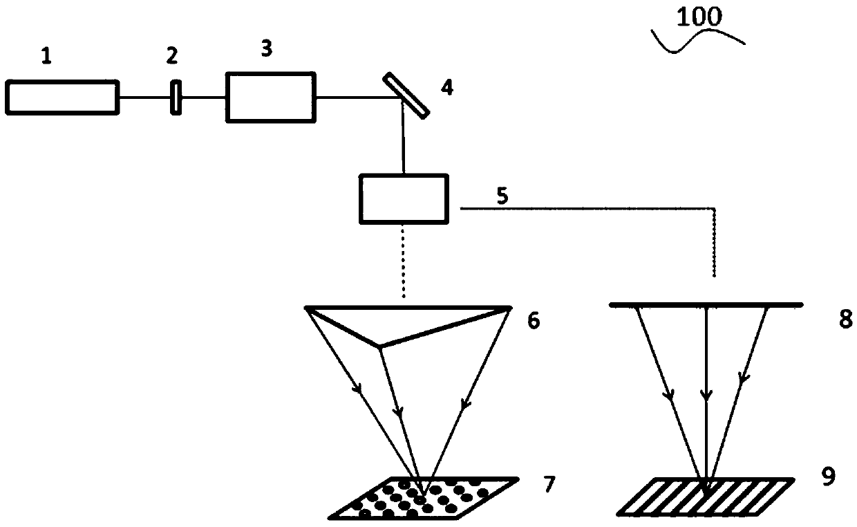
[0028] In order to enable those skilled in the art to better understand the solutions of the present invention, the following will clearly and completely describe the technical solutions in the embodiments of the present invention in conjunction with the drawings in the embodiments of the present invention. Obviously, the described embodiments are only It is an embodiment of a part of the present invention, but not all embodiments. Based on the embodiments of the present invention, all other embodiments obtained by persons of ordinary skill in the art without making creative efforts shall fall within the protection scope of the present invention.

[0029] The terms "first", "second", "third", "fourth", etc. (if any) in the description and claims of the present invention and the above drawings are used to distinguish similar objects and not necessarily Describe a particular order or sequence. It is to be understood that the terms so used are interchangeable under appropriate c...


PUM


Abstract

The embodiment of the invention discloses a system for manufacturing a modulation-free array structure by adopting a laser interference photoetching technology and a corresponding method. According tothe system, laser is adopted as a light-emitting light source; three coherent light beams are formed through shaping, collimation and beam splitting; the three coherent light beams converge and interfere on the plane of a substrate, so that light intensity is redistributed in an interference field, and therefore, periodic structures which are consistent in size and are uniformly distributed can be easily obtained. Modulation does not occur in a manufacturing process. The periodic pattern structure can be widely applied to the fields of functional surfaces, devices and the like.

Description

technical field [0001] The present invention relates to the technical field of laser interference lithography, in particular to a method for fabricating a non-modulation array structure using laser interference lithography technology, which can change the parameters of each beam of light arbitrarily and can ensure that the pattern distribution of the structure surface is periodic without modulation. system. Background technique [0002] Laser interference lithography is a technique for fabricating micro-nano patterns, which has attracted widespread attention due to its large area, high efficiency, and low cost. Laser interference lithography can produce micron-scale, nano-scale and micro-nano-mixed periodic patterns. For micro-nano-mixed periodic patterns, it can be realized by changing the incident angle or space angle of the incident light. Fabrication of periodic array patterns by laser interference lithography has attracted widespread attention because of its low cost a...

Claims


Application Information

Patent Timeline
Patent Type & Authority Applications(China)
IPC IPC(8): G03F7/20
CPCG03F7/70408
Inventor 徐佳张红鑫王泰升许文斌蔺春波王鹤刘建卓许家林
Owner CHANGCHUN INST OF OPTICS FINE MECHANICS & PHYSICS CHINESE ACAD OF SCI
Why Eureka
Try Eureka