Trench type MOS structure Schottky diode and preparation method thereof

A technology of Schottky diode and MOS structure, applied in the field of diodes, can solve the problems of increasing the reverse breakdown voltage of reverse leakage current, reducing the electric field strength of the Schottky surface, and reducing the forward conduction characteristics of the device.

Pending Publication Date: 2020-04-28
BYD SEMICON CO LTD +1
View PDF5 Cites 2 Cited by
  • Summary
  • Abstract
  • Description
  • Claims
  • Application Information

AI Technical Summary

Problems solved by technology

[0003] When the TMBS rectifier device is connected to the reverse bias voltage, the trench MOS structure is beneficial to reduce the electric field intensity on the surface of the Schottky, and suppresses the effect of reducing the barrier height of the Schottky barrier junction with the increase of the reverse bias voltage. Among them, The width and depth between the trenches have a significant impact on the reduction effect of the Schottky barrier. The narrower the width of the trench and the deeper the depth of the trench, the smaller the electric field intensity on the Schottky surface, which is conducive to the reverse of the device. The reduction of the leakage current and the increase of the reverse breakdown voltage, but the reduction of the width and the increase of the depth of the trench will reduce the forward conduction characteristics of the device and cause the increase of the on-resistance
[0004] Therefore, the research on Schottky diodes with trench-type MOS structures remains to be in-depth.

Method used


Image

  • Trench type MOS structure Schottky diode and preparation method thereof
  • Trench type MOS structure Schottky diode and preparation method thereof
  • Trench type MOS structure Schottky diode and preparation method thereof

Examples


Embodiment Construction

[0021] Embodiments of the present invention are described in detail below. The embodiments described below are exemplary and are only used for explaining the present invention, and should not be construed as limiting the present invention. Where specific techniques or conditions are not indicated in the examples, the techniques or conditions described in the literature in this field or the product specification shall be carried out.

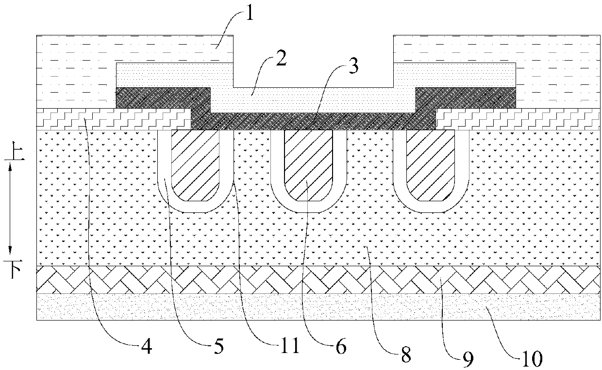
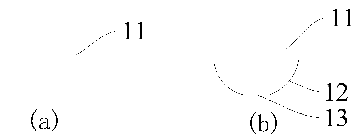
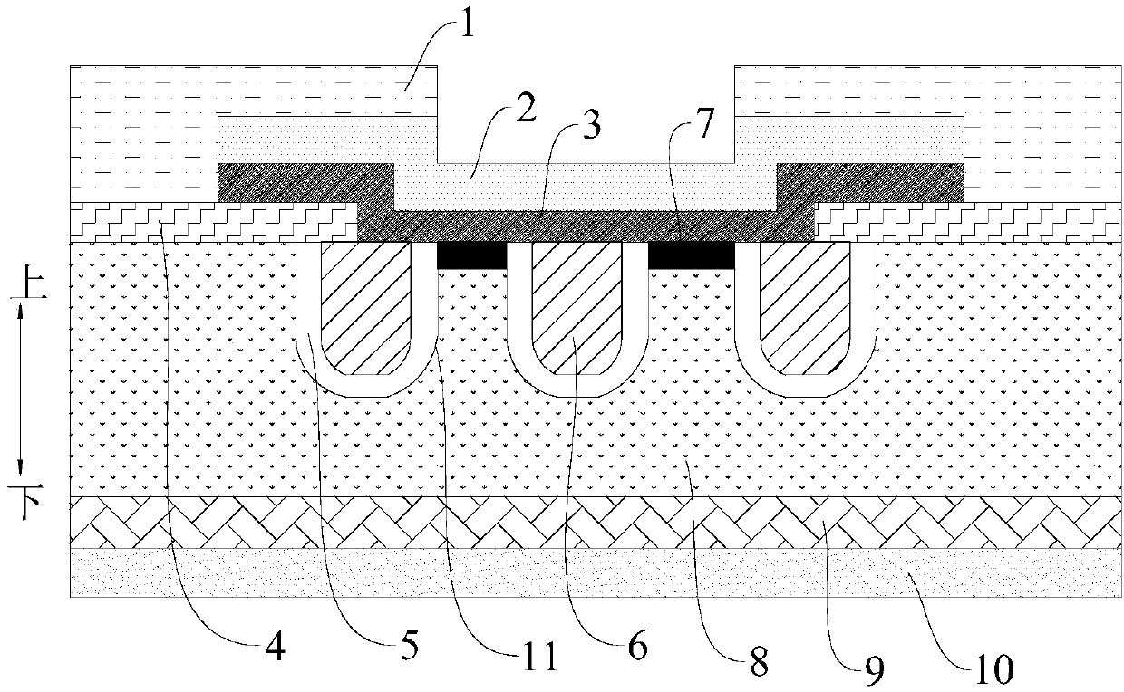
[0022] In one aspect of the present invention, the present invention provides a trench type MOS structure Schottky diode. According to an embodiment of the present invention, the trench type MOS structure Schottky diode includes an N-type doped substrate 9, an N-type doped epitaxial layer 8 arranged on the upper surface of the N-type doped substrate 9, and a The upper surface of the N-type doped epitaxial layer 8 extends toward a plurality of grooves 11 in the N-type doped epitaxial layer 8, wherein the doping concentration in the N-type doped e...


PUM

PropertyMeasurementUnit
thicknessaaaaaaaaaa
thicknessaaaaaaaaaa

Abstract

The invention provides a trench type MOS structure Schottky diode and a preparation method thereof. The trench type MOS structure Schottky diode comprises an N-type doped substrate, an N-type doped epitaxial layer arranged on the upper surface of the N-type doped substrate, and a plurality of trenches extending from the upper surface of the N-type doped epitaxial layer to the N-type doped epitaxial layer; doping concentration in the N-type doped epitaxial layer is gradually increased from top to bottom. Therefore, the impurity doping concentration of the N-type doped epitaxial layer in the Schottky diode is changed (the doping concentration in the N-type doped epitaxial layer is gradually increased from top to bottom); the electric field intensity distribution of the N-type doped epitaxiallayer can be changed, so that peak electric fields at the corners of the bottoms of the trenches are reduced; the reverse blocking characteristic of the Schottky diode and the forward conduction characteristic of the device are improved, namely, the reverse leakage current of the Schottky diode is reduced, and the reverse breakdown voltage of the Schottky diode is increased.

Description

technical field [0001] The present invention relates to the technical field of diodes, in particular to a trench type MOS structure Schottky diode and a preparation method thereof. Background technique [0002] At present, the trench type MOS structure Schottky diode (TMBS) uses the MOS structure to surround the Schottky barrier junction. By changing the electric field intensity distribution in the drift region between the MOS structures, the surface of the Schottky barrier junction in the drift region is suppressed. The peak electric field strength makes the peak electric field strength appear in the body of the device, thereby optimizing the forward and reverse electric parameter characteristics of the device. [0003] When the TMBS rectifier device is connected to the reverse bias voltage, the trench MOS structure is beneficial to reduce the electric field intensity on the surface of the Schottky, and suppresses the effect of reducing the barrier height of the Schottky ba...

Claims


Application Information

Patent Timeline
Patent Type & Authority Applications(China)
IPC IPC(8): H01L29/06H01L29/872H01L21/329
CPCH01L29/8725H01L29/66143H01L29/0684H01L29/0623
Inventor 王艳春周亮
Owner BYD SEMICON CO LTD
Why Eureka
Try Eureka