A new type of large-diameter semiconductor chip and molybdenum sheet bonding ohmic contact processing method

A technology of ohmic contact and processing method, which is applied in the direction of semiconductor devices, semiconductor/solid-state device manufacturing, electric solid-state devices, etc., can solve the deterioration of electrical characteristic parameters, change the PN junction depth and surface concentration distribution, and have large contact transient thermal resistance and other issues, to achieve the effect of improving consistency and yield, improving reverse blocking characteristics, and improving flow capacity

Active Publication Date: 2017-10-31
西安派瑞功率半导体变流技术股份有限公司
View PDF3 Cites 0 Cited by
  • Summary
  • Abstract
  • Description
  • Claims
  • Application Information

AI Technical Summary

Problems solved by technology

[0004] 1) Since the process temperature is as high as 700°C, the thermal expansion coefficients of Si and Mo are inconsistent, and large deformation occurs after cooling, which causes stress inside the chip, which may lead to increased pressure drop, poor contact of the electric heating circuit, and poor heat dissipation. The chip is broken when it is subjected to electric heat or mechanical shock, making the device permanently invalid
[0005] 2) Using the mutual fusion of Si and Al at high temperature, the formation of an alloy layer will consume a certain depth of silicon on the surface, unevenly change the original PN junction depth and surface concentration distribution, and deteriorate the electrical characteristic parameters
[0006] 3) In the process of high temperature, AL first turns into a liquid, which is easy to lose, resulting in edge voids and other local adhesion problems, and does not form an excellent ohmic contact, resulting in a decrease in blocking voltage, an increase in on-state voltage drop, a decrease in flow capacity, and heat dissipation. poor effect
The disadvantage is that the contact transient thermal resistance is large and the surge current is small

Method used


Image

  • A new type of large-diameter semiconductor chip and molybdenum sheet bonding ohmic contact processing method
  • A new type of large-diameter semiconductor chip and molybdenum sheet bonding ohmic contact processing method
  • A new type of large-diameter semiconductor chip and molybdenum sheet bonding ohmic contact processing method

Examples


Embodiment Construction

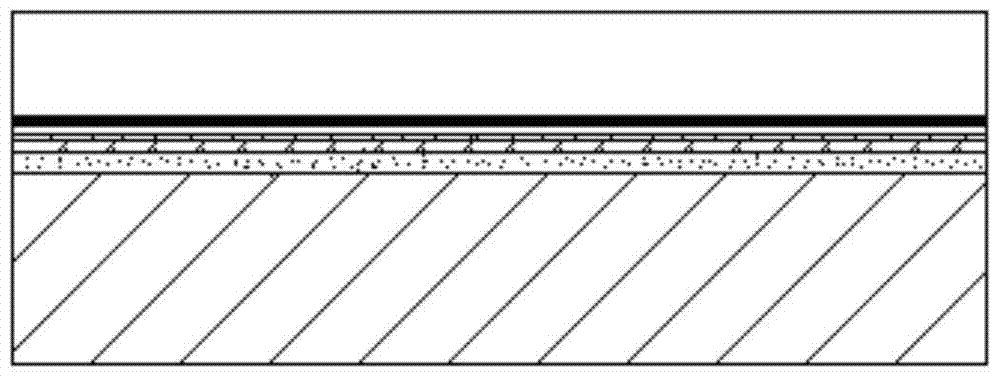
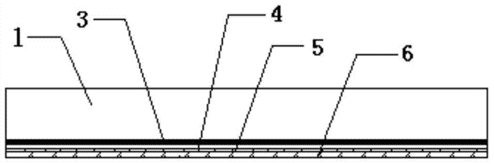
[0028] A new type of large-diameter semiconductor chip and molybdenum sheet bonding ohmic contact processing method, including semiconductor chip 1, molybdenum sheet 2, and the contact layers between semiconductor chip 1 and molybdenum sheet 2 respectively have Al electrode layer 3, Ti / Pt / Au Metal transition layers 4, 5, 6, Ag layer solder layer 7, immerse the semiconductor chip 1 with a 10 μm AL layer 3 on the anode steamed into dilute hydrofluoric acid with a volume ratio of 1±0.5% and the composition is ammonia water: hydrogen peroxide: pure water volume ratio 1:2:5 cleaning solution 1#, then put it in a clean oven and dry it at 100±2℃. Go through the following steps in order:

[0029] First, when the vacuum degree is higher than 1×10 -5 Pa, at a temperature of 100±2°C, bombard the Ti source in the crucible with an electron beam above 10000EV (electron volts), so that the Ti source is excited into a gaseous state, which is evenly distributed in the evaporation chamber in t...


PUM


Abstract

The invention provides a novel large diameter semiconductor chip and molybdenum sheet bonding type ohmic contact processing method. A semiconductor chip and a molybdenum sheet are comprised. Contact layers between the semiconductor chip and the molybdenum sheet comprise Al electrode layer, a Ti / Pt / Au metal transition layer and an Ag solder layer. According to the invention, a number of metal transition layers and the solder layer are introduced; a metal atom micro diffusion bonding principle is used; the characteristics of low conductivity and easy bonding with other metal at a low temperature of Au and Ag are used, so that the semiconductor chip Si and the Mo sheet are firmly adhered together to form a great ohmic contact technology; the high power semiconductor chip and the molybdenum sheet form large area ohmic contact without deformation; the on-state voltage drop of a device is significantly reduced; the flow capacity, the reverse blocking characteristic and the heat radiating effect of the device are improved; the parameter consistency and the yield of the device are improved; and huge economic benefits are produced.

Description

technical field [0001] The invention relates to the technical field of manufacturing power semiconductor devices, in particular to a processing method for a high-power thyristor, a rectifier semiconductor chip and a molybdenum sheet bonding ohmic contact technology. Background technique [0002] As we all know, high-power thyristors and rectifiers are power semiconductor discrete devices, and their development direction is high-voltage and high-current power, and the chip area is relatively large. During operation, it bears high voltage and generates a lot of heat through high current, which needs to be carried away by metal electrode conduction. The tightness of the contact between the metal electrode and the semiconductor chip and the flatness of the interface determine the electrothermal resistance and flow capacity of the device. [0003] The existing contact technologies between high-power discrete device chips and molybdenum sheets (electrodes) include high-temperatur...

Claims


Application Information

Patent Timeline
Patent Type & Authority Patents(China)
IPC IPC(8): H01L21/60
CPCH01L24/84
Inventor 高山城周哲赵卫
Owner 西安派瑞功率半导体变流技术股份有限公司
Why Eureka
Try Eureka