New device and method for simultaneous quasi-aplanatic imaging confocal detection of adjacent surfaces of semiconductor crystal grains

An imaging detection and semiconductor technology, which is used in measurement devices, optical testing of flaws/defects, and material analysis by optical means, can solve problems such as increasing the difficulty of implementing detection systems, and achieve compact structure, small size, and convenient use.

Pending Publication Date: 2020-05-01
QUANZHOU NORMAL UNIV
View PDF3 Cites 4 Cited by
  • Summary
  • Abstract
  • Description
  • Claims
  • Application Information

AI Technical Summary

Problems solved by technology

[0008] In the scheme proposed by the applicant in previous patent applications (patent application numbers 201910207016.2, 201911247575.2), since the optical path difference △ of double-sided simultaneous imaging detection is related to the structural parameters (L1, L2), when the structural parameters are large, the method Inevitably there are certain limitations in use; the above two applications use a larger right-angle transfer prism and a large depth-of-field telecentric imaging lens to solve the resolution problems caused by simultaneous detection of adjacent surfaces and their optical path diffe

Method used


Image

  • New device and method for simultaneous quasi-aplanatic imaging confocal detection of adjacent surfaces of semiconductor crystal grains
  • New device and method for simultaneous quasi-aplanatic imaging confocal detection of adjacent surfaces of semiconductor crystal grains
  • New device and method for simultaneous quasi-aplanatic imaging confocal detection of adjacent surfaces of semiconductor crystal grains

Examples


Embodiment Construction

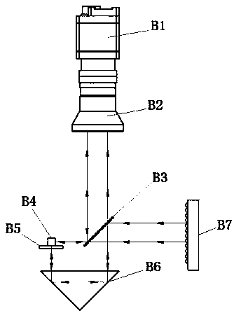
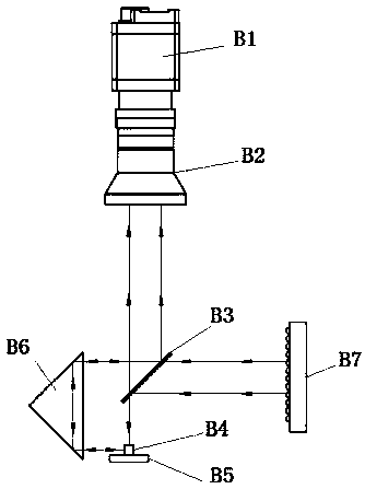
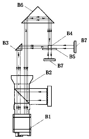
[0049] The novel device for simultaneously quasi-equal optical path confocal imaging detection of adjacent surfaces of semiconductor crystal grains of the present invention includes a camera 1, a telecentric imaging lens 2, a semi-transparent and semi-reflective image combiner 3, and a semiconductor grain 6 arranged in sequence in the direction of the optical path And be used for carrying the transparent stage 5 of semiconductor crystal grain, on the optical path between semiconductor crystal grain 6 and transflective image combiner 3, be respectively provided with the first right angle relay prism 4b and the second right angle relay image Prism 4a, the first right-angle transfer prism 4b and the second right-angle transfer prism 4a are located at the peripheral side of the semiconductor crystal grain 6, and the first right-angle transfer prism 4b and the semi-transparent and half-reflection image combiner 3 are located at the telecentric imaging lens 2 on the optical axis A, a...


PUM


Abstract

The invention discloses a new method for simultaneous quasi-aplanatic imaging confocal detection of adjacent surfaces of semiconductor crystal grains. A detection device comprises a camera, a telecentric imaging lens, a semi-transparent and semi-reflective image combiner, the semiconductor crystal grains and a transparent object stage for bearing the semiconductor crystal grains which are sequentially arranged in a direction of a light path; a first right-angle transferring prism and a second right-angle transferring prism are respectively arranged on the light path between the semiconductor crystal grains and the semi-transparent and semi-reflective image combiner, the second right-angle transferring prism is positioned at a first side part of the optical axis of the telecentric imaging lens, the two right-angle surfaces of the two right-angle transferring prisms are respectively vertical to the light path, at least two surfaces of the semiconductor crystal grains are respectively imaged at different area positions on a sensor surface of the camera through the right-angle transferring prisms and the semi-transparent and semi-reflective image combiner by double light paths, and thedistance delta between the double images of the adjacent surfaces is adjustable.

Description

Technical field: [0001] The invention belongs to the fields of optical detection and machine vision, and in particular relates to a new device and method for simultaneous quasi-equal optical path confocal imaging detection of adjacent surfaces of semiconductor crystal grains. Background technique: [0002] In the application of machine vision imaging inspection, when the object to be inspected is large, a telecentric imaging lens with a suitable field of view is usually selected at one station to inspect one surface of the object; when the object to be inspected is small (such as semiconductor optoelectronic components) , in order to improve the detection speed and make full use of the effective field of view of the telecentric imaging lens, a technical solution of simultaneously detecting two surfaces of the object with one telecentric imaging lens on one station is adopted. [0003] The main technical problems to be solved by the device and method for simultaneous defect d...

Claims


Application Information

Patent Timeline
IPC IPC(8): G01N21/01G01N21/95
CPCG01N21/01G01N21/9505
Inventor 廖廷俤陈武付宝玉
Owner QUANZHOU NORMAL UNIV
Why Eureka
Try Eureka