Terahertz frequency band passive device design method

A technology of passive devices and design methods, applied in the direction of CAD circuit design, etc., can solve the problems of inefficiency, cumbersome, time-consuming, etc., and achieve the effect of simplifying the design process, high circuit processing accuracy, and easy scaling process

Active Publication Date: 2020-05-01
UNIV OF ELECTRONICS SCI & TECH OF CHINA
View PDF8 Cites 0 Cited by
  • Summary
  • Abstract
  • Description
  • Claims
  • Application Information

AI Technical Summary

Problems solved by technology

However, when designing the same passive components in other frequency bands, such an implicit relationship is not utilized, and the inefficient, cumbersome and time-consuming design process is still repeated.

Method used


Image

  • Terahertz frequency band passive device design method
  • Terahertz frequency band passive device design method
  • Terahertz frequency band passive device design method

Examples


Embodiment 1

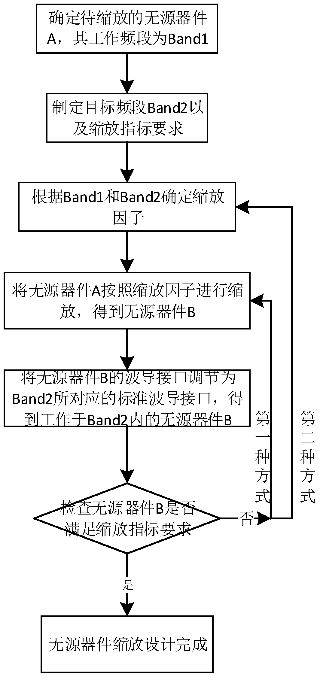
[0039] Please refer to figure 1 and figure 2 , the present embodiment provides a method for designing passive devices in the terahertz frequency band, including the following steps:

[0040] S1. Determine the passive device A to be scaled, and its working frequency band is Band1.

[0041] In this embodiment, the passive device A is a device that has been designed according to the traditional method. The traditional method refers to scanning parameters one by one or multi-parameter optimization design, etc. The passive device A can be a filter, a power splitter, a transition conversion Wait.

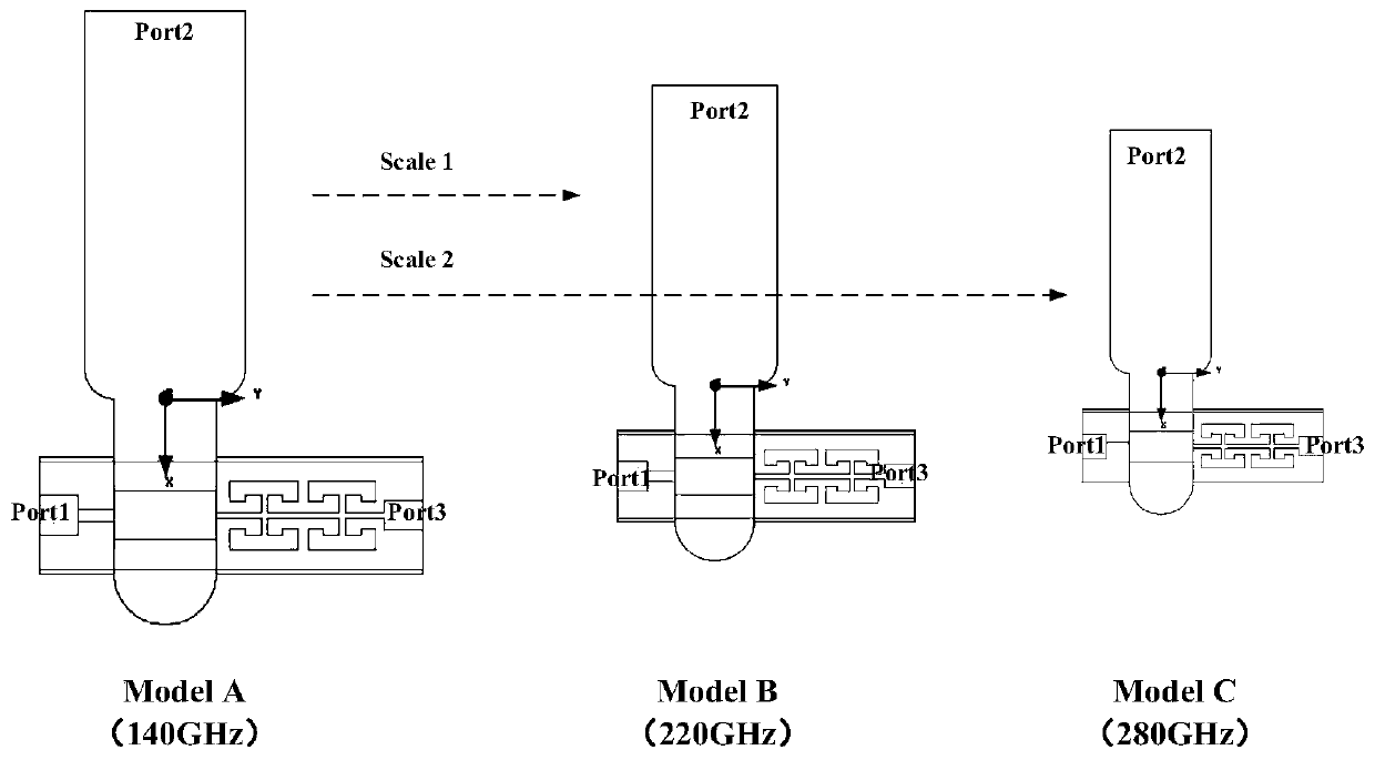
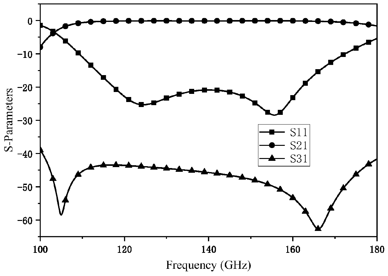
[0042] In this embodiment, the passive device A selects Model A, and Model A is an E-plane probe transition structure with a center frequency of 140 GHz and a DC bias filter, and its substrate is a quartz substrate with a substrate thickness of 50 μm. The waveguide is WR6.5 (1.651mm×0.826mm), and the simulation results are as follows image 3 shown, from image 3 It can be seen that...

Embodiment 2

[0056] Please refer to figure 1 and figure 2 , compared with Example 1, Model A is still used as passive device A, but the difference is that the target frequency band Band2 is 230-330GHz, the scaling index is required to be within the frequency range of 230-330GHz, the return loss is better than 20dB, and the insertion loss Better than 0.25dB; in the frequency range of 205-360GHz, the isolation between DC and RF ports is better than 40dB.

[0057] In this embodiment, a passive device B working at 280 GHz is obtained. The passive device B is Model C, wherein the scaling factor is 0.5 (1×140 / 280), the thickness of the quartz substrate is 30 um, and the output interface is WR3. 4 (0.864mm×0.432mm). The simulation results of Model C are as follows Figure 5 It can be seen from the figure that the center frequency of Model C is 280GHz, and in the frequency range of 230-330GHz, the return loss is better than 20dB, and the insertion loss is better than 0.25dB; in the frequency r...


PUM


Abstract

The invention discloses a terahertz frequency band passive device design method which comprises the following steps: determining a passive device A to be zoomed and a working frequency band of the passive device A to be zoomed as Band1; formulating a target frequency band Band2 and zoom index requirements; determining a scaling factor eta according to the central frequency relationship between theBand1 and the Band2; scaling the passive device A according to the scaling factor eta to obtain a passive device B; adjusting a waveguide interface of the passive device B to a standard waveguide interface corresponding to the Band2 to obtain a passive device B working in the Band2; and checking whether the passive device B meets the zoom index requirement or not. The designed passive device is reasonably scaled, and the internal structure-frequency dependence relationship of the device is fully utilized, so that the passive device can work in any required frequency band; the invention is simple and easy and convenient to operate, the design process of the terahertz frequency band passive device is greatly simplified, and the method has good practical value in design of functional circuits such as a terahertz frequency multiplier, a frequency mixer, a detector and an amplifier.

Description

technical field [0001] The invention relates to the technical field of passive device design, in particular to a method for designing passive devices in the terahertz frequency band. Background technique [0002] Terahertz frequency multipliers, mixers, detectors, amplifiers and other functional circuits require the support of various passive components, including signal transmission, filtering, transition, etc. The design of these passive components needs to rely on the establishment of corresponding passive structure models in high-frequency finite element simulation software such as HFSS and full-wave simulation. The design goal of the process is clear, and the model has good versatility. However, in the process of simulation, it is necessary to continuously scan and optimize parameters until the design goal is achieved. Due to the high frequency of terahertz, when the passive structure is relatively complex, the mesh division of the passive structure by the simulation ...

Claims


Application Information

Patent Timeline
Patent Type & Authority Applications(China)
IPC IPC(8): G06F30/39
Inventor 张勇吴成凯汪涵魏浩淼胡江延波徐锐敏
Owner UNIV OF ELECTRONICS SCI & TECH OF CHINA
Why Eureka
Try Eureka