Fingerprint recognition device and electronic equipment

A fingerprint identification and fingerprint technology, which is applied in radiation control devices, character and pattern recognition, and acquisition/organization of fingerprints/palmprints. The problem of small amount of light entering the device can achieve the effect of facilitating layout and routing, reducing exposure time, and improving recognition problems

Active Publication Date: 2020-05-01
SHENZHEN GOODIX TECH CO LTD
View PDF28 Cites 3 Cited by
  • Summary
  • Abstract
  • Description
  • Claims
  • Application Information

AI Technical Summary

Problems solved by technology

With this technical solution, the overall light input of the fingerprint recognition device is small, the exposure time is long, the overall imaging quality is poor, and the recognition performance for dry fingers is not good.
At the same time, the thickness of the optical path in the fingerprint identification device is thick, which increases the processing difficulty and cost of the optical path, and is not conducive to the development of thinner and lighter fingerprint identification devices.

Method used


Image

  • Fingerprint recognition device and electronic equipment
  • Fingerprint recognition device and electronic equipment
  • Fingerprint recognition device and electronic equipment

Examples


Embodiment Construction

[0081] The technical solutions in the embodiments of the present application will be described below with reference to the accompanying drawings.

[0082] It should be understood that the embodiments of the present application can be applied to optical fingerprint systems, including but not limited to optical fingerprint recognition systems and products based on optical fingerprint imaging. The examples constitute no limitations, and the embodiments of the present application are also applicable to other systems using optical imaging technology.

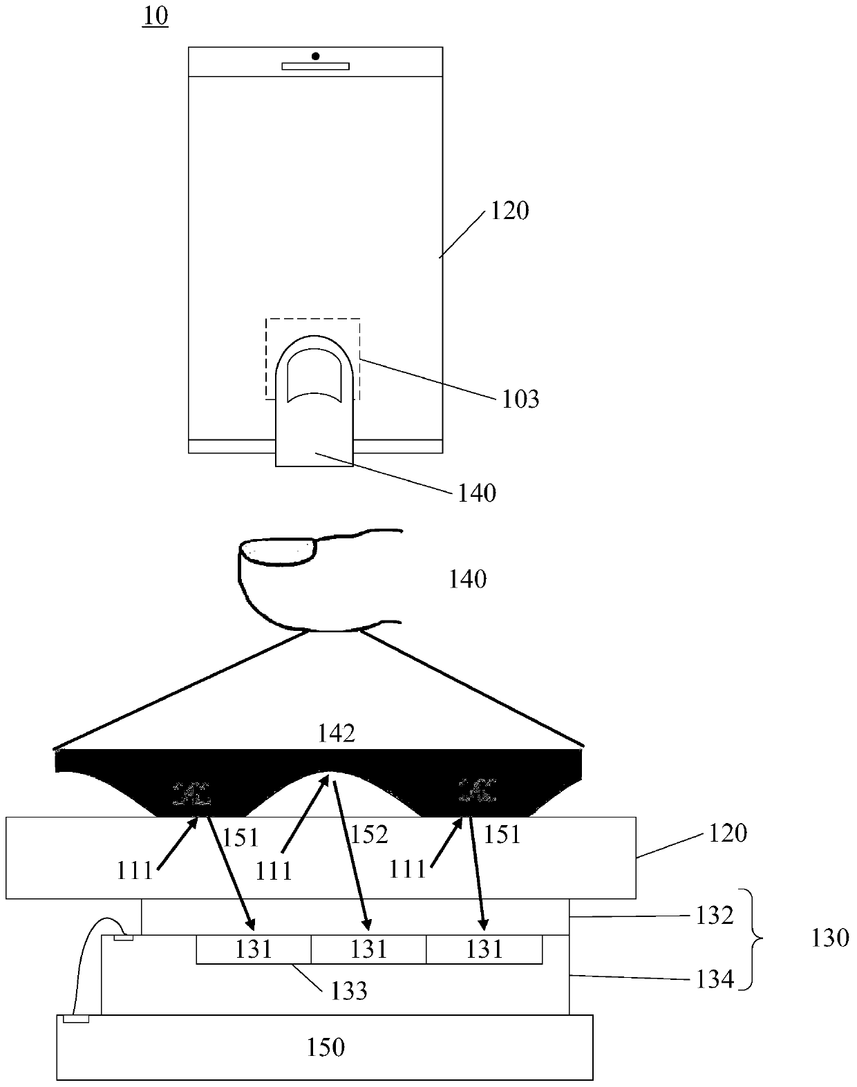
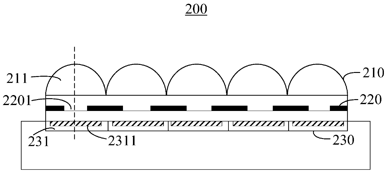
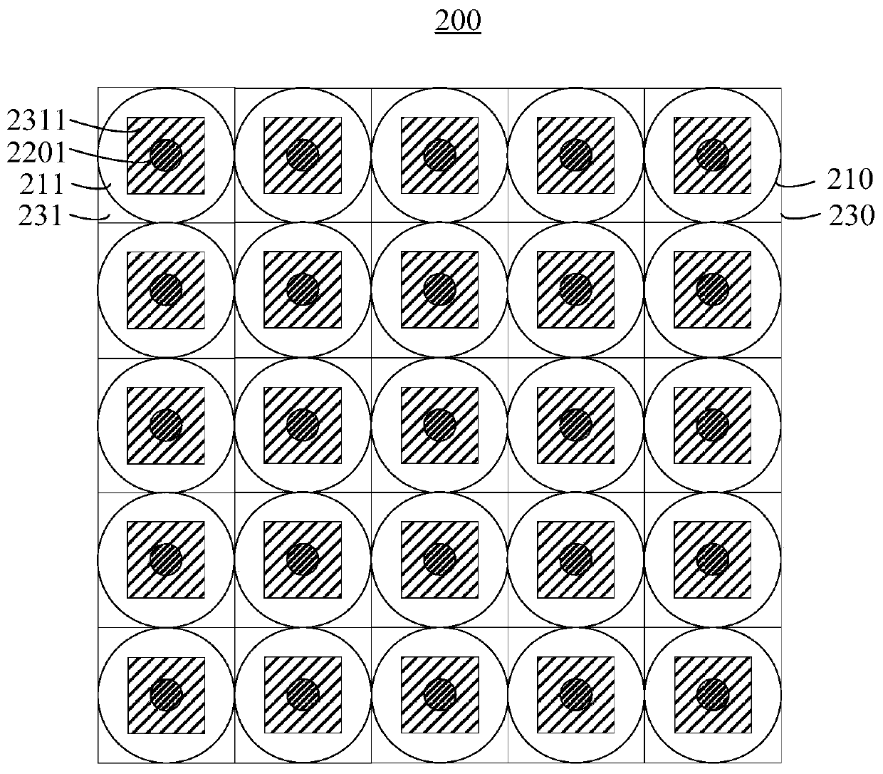
[0083] As a common application scenario, the optical fingerprint system provided by the embodiment of this application can be applied to smartphones, tablet computers, and other mobile terminals with display screens or other electronic devices; more specifically, in the above electronic devices, fingerprint recognition The device may specifically be an optical fingerprint device, which may be arranged in a partial or entire area unde...


PUM


Abstract

The embodiment of the invention discloses a fingerprint recognition device and electronic equipment. The performance of the fingerprint recognition device can be improved. The fingerprint recognitiondevice is suitable for being arranged below a display screen to realize optical fingerprint recognition under the screen, the fingerprint recognition device comprises a plurality of fingerprint recognition units, and each fingerprint recognition unit comprises a micro lens; at least two light blocking layers, wherein each light blocking layer is provided with a light through hole to form two lightguide channels in different directions; the two pixel units are respectively positioned at the bottoms of the two light guide channels; wherein after fingerprint optical signals returned from a finger above the display screen are converged through the micro lens, two target fingerprint optical signals in different directions are transmitted to the two pixel units through the two light guide channels respectively. A plurality of groups of two pixel units in the fingerprint recognition device receive fingerprint optical signals in two different directions and convert the fingerprint optical signals into two fingerprint images, the two fingerprint images are moved and reconstructed into a reconstructed image, and the reconstructed image is used for fingerprint recognition.

Description

[0001] This application claims priority from the following applications, the entire contents of which are hereby incorporated by application: [0002] On August 23, 2019, a PCT application with the application number PCT / CN2019 / 102366 and the title of the invention "fingerprint detection device, method and electronic equipment" was submitted to the China Patent Office; [0003] On October 18, 2019, a PCT application with the application number PCT / CN2019 / 111978 and the title of the invention "Fingerprint Detection Device and Electronic Equipment" was submitted to the China Patent Office. technical field [0004] The present application relates to the technical field of fingerprint identification, and more specifically, to a fingerprint identification device and electronic equipment. Background technique [0005] With the rapid development of the terminal industry, people pay more and more attention to biometric technology, and the more convenient off-screen biometric technol...

Claims


Application Information

Patent Timeline
Patent Type & Authority Applications(China)
IPC IPC(8): G06K9/00H01L27/146
CPCH01L27/14625H01L27/14627H01L27/14623G06V40/1324G06V40/1318H01L2224/48091H01L2924/00014
Inventor 蒋鹏马明
Owner SHENZHEN GOODIX TECH CO LTD
Why Eureka
Try Eureka