Two-dimensional adjustable terahertz photoconductive antenna

A photoconductive antenna and terahertz technology, which is applied in the field of terahertz optoelectronic devices, can solve the problems of inability to ensure no gaps, inability to optimize silicon lenses, and inability to replace the success rate of photoconductive antenna assembly, so as to reduce the risk of crushing and improve assembly success. rate effect

Inactive Publication Date: 2020-05-05
DAHENG NEW EPOCH TECH
View PDF7 Cites 0 Cited by
  • Summary
  • Abstract
  • Description
  • Claims
  • Application Information

AI Technical Summary

Problems solved by technology

Although the photoconductive antenna assembled by this method is small in size, it also has many defects, such as the inability to optimize the position of the silicon lens in the optical path, the inability to replace the photoconductive antenna, and the low assembly success rate (mainly because it cannot guarantee There is no gap between the silicon lens and the photoconductive antenna) etc.

Method used


Image

  • Two-dimensional adjustable terahertz photoconductive antenna
  • Two-dimensional adjustable terahertz photoconductive antenna
  • Two-dimensional adjustable terahertz photoconductive antenna

Examples


Embodiment 1

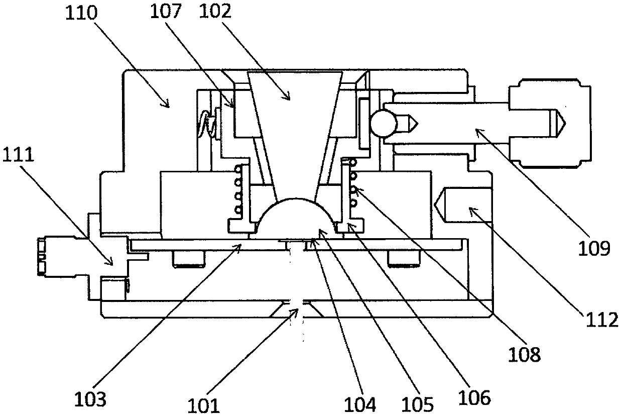
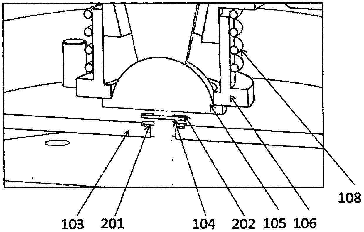
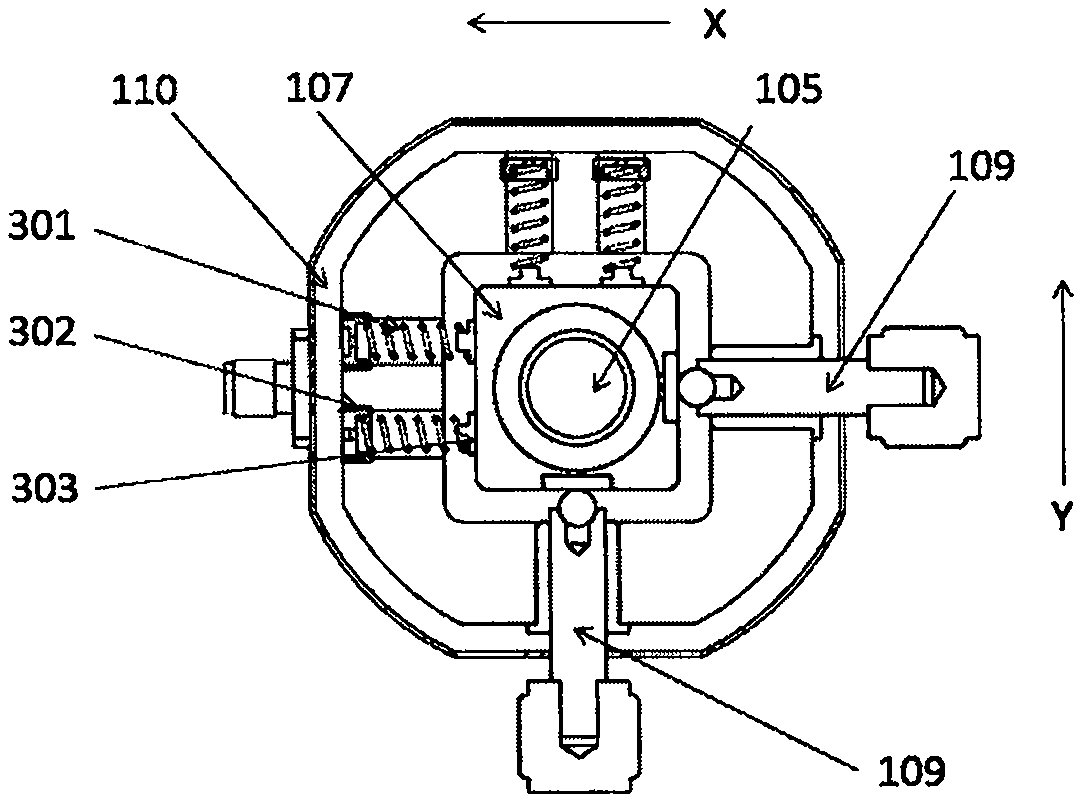
[0022] figure 1 is a schematic diagram of the terahertz photoconductive antenna of the present invention. The femtosecond pulsed laser 101 passes through the hole on the circuit board 103 and then focuses on the metal electrode of the 104 terahertz chip, and the generated terahertz wave 102 is emitted after passing through the 105 silicon lens. In practical applications, the terahertz chip 104 is placed on the circuit 103, and the silicon lens 105 is pressed together with the terahertz chip. Since the laser beam needs to hit the center of the silicon lens accurately before being emitted, it is necessary to adjust the position of the silicon lens 105 to ensure the centering of the laser beam. In the present invention, a spring 108 is placed between the adapter body 106 and the movable unit 107 to ensure that the terahertz chip, the circuit board, and the silicon lens are pressed together. The movable unit 107 can be driven by 109 integral screws to realize X-Y two-dimensional...


PUM


Abstract

The invention discloses a two-dimensional adjustable terahertz photoconductive antenna which comprises a body structure, a movable unit, a silicon lens, an adapter, a terahertz chip, a circuit board and the like. The silicon lens with a boss, the terahertz chip and the circuit board are pressed together through a mechanical structure with a spring to form the complete terahertz photoconductive antenna. The position of the silicon lens can be adjusted by rotating an adjusting screw so that a signal generated by the terahertz chip is optimal. The two-dimensional adjustable terahertz antenna is compact in structure mode and stable in adjusting process, the user can conveniently operate to obtain the optimal terahertz wave signal, and the terahertz antenna has high integration degree and integration and industrialization of a terahertz time domain spectrometer are facilitated.

Description

technical field [0001] The invention relates to the technical field of terahertz optoelectronic devices, in particular to a photoconductive antenna integrated device for generating and detecting terahertz waves in a terahertz spectrum measurement system. Background technique [0002] Terahertz waves generally refer to electromagnetic waves with a frequency between 0.1-10THz, and their wavelength is in the range of 0.03-3mm, which is between microwave and infrared. This band is in a special position in the electromagnetic spectrum, and the related theory is in the transition zone between macroscopic electromagnetism and microphotonics. Compared with traditional light sources, terahertz waves have many unique advantages such as transient, low energy, broadband and coherence. At the same time, terahertz spectroscopy has been applied to more and more fields due to its excellent properties such as strong transmittance, high resolution, and sensitivity to interactions with biolog...

Claims


Application Information

Patent Timeline
IPC IPC(8): G02B6/124
CPCG02B6/1245G02B2006/12061G02B2006/12102
Inventor 冯忠磊张翼邓朝
Owner DAHENG NEW EPOCH TECH
Why Eureka
Try Eureka