

OTP memory and manufacturing method thereof
一种制造方法、存储器的技术,应用在只读存储器、静态存储器、半导体/固态器件制造等方向,能够解决不利千位元等级高密度的应用、存储单元面积大等问题,达到读取操作简单且快速、提高写入速度的效果
- Summary
- Abstract
- Description
- Claims
- Application Information
AI Technical Summary
Problems solved by technology
Method used
Image

Examples
Embodiment Construction
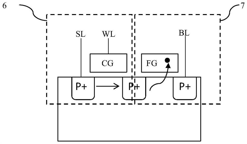
[0068] like Figure 4 shown, is the layout of the OTP memory according to the embodiment of the present invention; as Figure 5 shown, is the embodiment of the present invention OTP memory edge Figure 4 The cross-sectional view of the AA line; the cell structure of the OTP memory according to the embodiment of the present invention includes: a first active region 201 and a second active region 202 .
[0069] The first active region 201 and the second active region 202 intersect vertically.
[0070] EDNMOS is formed in the first active region 201 , and PMOS is formed in the second active region 202 .
[0071] The EDNMOS includes a first source region 205, a first channel region 206, a drift region 207, a first drain region 209 and a first gate structure, and the first gate structure consists of a first gate dielectric layer 214a and a first gate dielectric layer 214a. The polysilicon gate 203 is superimposed, the direction between the first source region 205 and the first d...
PUM
 Abstract
Description
Claims
Application Information