PDMS/SiC functional gradient substrate and preparation method and application thereof

A functional gradient and substrate technology, applied in semiconductor/solid-state device manufacturing, manufacturing tools, additive manufacturing, etc., can solve the problem of damage to connected circuits and embedded electronic components, difficulty in the normal operation of flexible electronic products, and restrictions on the performance and function of flexible electronics, etc. problem, to achieve the effect of reducing processing steps, ensuring performance, and small thermal expansion coefficient

Active Publication Date: 2020-05-15
QINGDAO TECHNOLOGICAL UNIVERSITY
View PDF18 Cites 3 Cited by
  • Summary
  • Abstract
  • Description
  • Claims
  • Application Information

AI Technical Summary

Problems solved by technology

However, existing substrates have obvious deficiencies and inherent defects. For example, when flexible electronic products undergo excessive deformation, traditional single-material homogeneous substrates will easily cause damage to connecting circuits and embedded electronic components, resulting in Flexible electronic products are difficult to work properly and even cause them to fail
In addition, with the enhancement of device functions, the number of embedded electronic components continues to increase, and the heat generation of flexible electronics is also increasing. However, the heat dissipation performance of existing substrate materials is generally poor (low thermal conductivity), resulting in electronic components The life is shortened, the performance is unstable or even burned out, the stability and reliability are deteriorated, and it also restricts the further improvement and improvement of the performance and functions of flexible electronics and other products.
In particular, the traditional single-material substrate cannot solve the problem of having good flexibility and high rigidity at the same time.

Method used


Image

  • PDMS/SiC functional gradient substrate and preparation method and application thereof
  • PDMS/SiC functional gradient substrate and preparation method and application thereof
  • PDMS/SiC functional gradient substrate and preparation method and application thereof

Examples


Embodiment 1

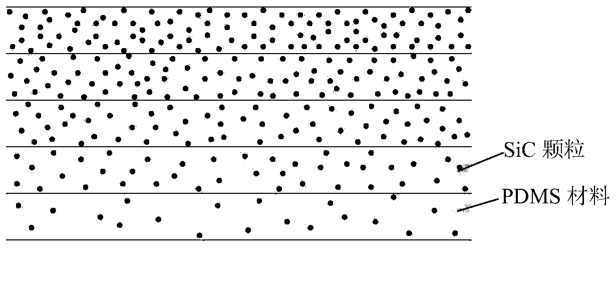
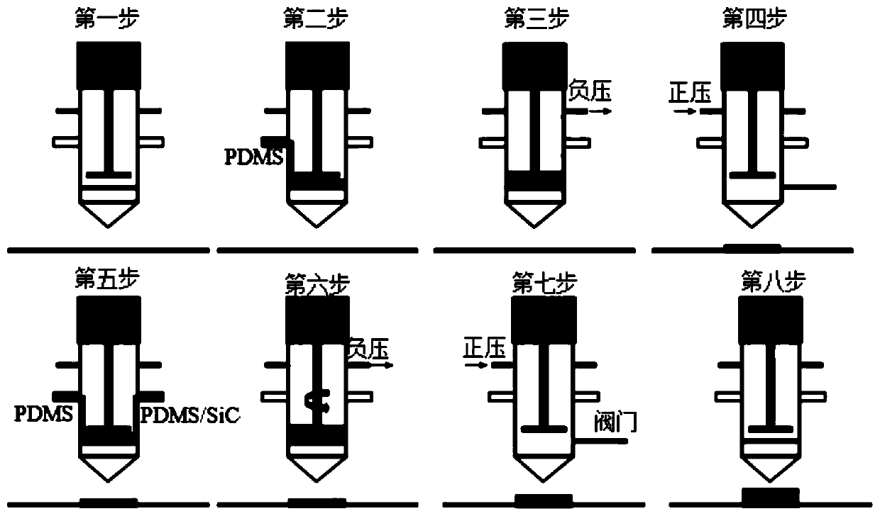
[0048] Such as figure 2 As shown, the specific method of PDMS / SiC functionally graded substrate:

[0049] Step 1: Printing material I and printing material II pretreatment. After uniformly mixing PDMS and curing agent at a ratio of 10:1 and vacuuming to remove air bubbles, it is used as the raw material of the feeding module I (printing material I). First, pure PDMS is prepared according to the ratio of PDMS and curing agent 10:1, and then the PDMS-SiC-curing agent mixture (printing material II) is prepared according to the silicon content of 50%. During the preparation process, the PDMS-SiC - Mix the curing agent mixture evenly.

[0050] Step 2: Pre-printing processing. Put the configured printing material I into the feeding device I, and put the processed printing material II into the feeding device II; the printing platform is heated to 80°C; the printing nozzle and the printing platform move to the initial printing position (i.e. print origin), complete the preparatio...

Embodiment 2

[0060] Such as figure 2 As shown, the specific method of PDMS / SiC functionally graded substrate:

[0061] Step 1: Printing material I and printing material II pretreatment. After uniformly mixing PDMS and curing agent according to 9:1 and vacuuming, it is used as the raw material of feeding module I (printing material I). First, pure PDMS is prepared according to the ratio of PDMS and curing agent 10:1, and then the PDMS-SiC-curing agent mixture (printing material II) is prepared according to the silicon content of 40%. During the preparation process, the PDMS-SiC - Mix the curing agent mixture evenly.

[0062] Step 2: Pre-printing processing. Put the configured printing material I into the feeding device I, and put the processed printing material II into the feeding device II; the printing platform is heated to 80°C; the printing nozzle and the printing platform move to the initial printing position (i.e. print origin), complete the preparations.

[0063] Step 3: Print....

Embodiment 3

[0069] Such as figure 2 As shown, the specific method of PDMS / SiC functionally graded substrate:

[0070] Step 1: Printing material I and printing material II pretreatment. After uniformly mixing PDMS and curing agent according to 10:1 and evacuating, it is used as the raw material of feeding module I (printing material I). First, pure PDMS is prepared according to the ratio of PDMS and curing agent 10:1, and then the PDMS-SiC-curing agent mixture (printing material II) is prepared according to the silicon content of 30%. During the preparation process, the PDMS-SiC - Mix the curing agent mixture evenly.

[0071] Step 2: Pre-printing processing. Put the configured printing material I into the feeding device I, and put the processed printing material II into the feeding device II; the printing platform is heated to 75°C; the printing nozzle and the printing platform move to the initial printing position (i.e. print origin), complete the preparations.

[0072] Step 3: Prin...


PUM

PropertyMeasurementUnit
heightaaaaaaaaaa
particle sizeaaaaaaaaaa
thermal conductivityaaaaaaaaaa

Abstract

The invention discloses a PDMS/SiC functional gradient substrate and a preparation method and an application thereof. PDMS in the substrate is a matrix material and SiC is a reinforcing phase; the SiCcontent is in gradient increasing from the outside of the substrate to the inside of the substrate, and the minimum value of SiC content on the outside of the substrate is 0-5%, the maximum value ofthe SiC content in the substrate is 45-55%, -55%, wherein the inner side of the substrate is one side used for being inserted into an electronic component and a connecting circuit. The rigidity of thesubstrate gradually increases from the outer surface to the inner surface, and the flexibility gradually decreases. Namely, the good flexibility on the outer surface of the substrate ensures that thesurface has very good conformability and stretchable/bendable characteristics to meet the requirements of actual working environment and use conditions; however, one side of the inner surface of thesubstrate has higher rigidity, so as to avoid the damage of the electronic component and the connecting circuit caused by excessive deformation when placing the electronic component and printing the connecting circuit (the excessive deformation is limited by improving rigidity constraint), and the stable electrical performance of the electronic component is ensured.

Description

technical field [0001] The invention belongs to the technical field of flexible electronics and additive manufacturing, and in particular relates to a PDMS / SiC functionally graded substrate and a preparation method and application thereof. Background technique [0002] The information disclosed in this background section is only intended to increase the understanding of the general background of the present invention, and is not necessarily taken as an acknowledgment or any form of suggestion that the information constitutes the prior art already known to those skilled in the art. [0003] Flexible electronics is an emerging electronic technology that makes organic / inorganic material electronic devices on flexible / ductile or bendable substrates (substrates), and it has been used in flexible displays, OLEDs, flexible solar cells, stretchable electronics, electronic Skin, wearable electronic devices, implantable medical electronics, soft robots and many other fields show broad...

Claims


Application Information

Patent Timeline
Patent Type & Authority Applications(China)
IPC IPC(8): B29C64/112H01L51/50H01L31/0392H01L31/0445B33Y10/00B33Y70/10B33Y80/00
CPCB29C64/112H01L31/03926H01L31/0445B33Y10/00B33Y70/00B33Y80/00H10K77/111H10K50/00Y02E10/549
Inventor 兰红波杨建军张源值朱晓阳齐田宇周龙健
Owner QINGDAO TECHNOLOGICAL UNIVERSITY
Why Eureka
Try Eureka