Novel two-dimensional heterojunction material and preparation method thereof

A two-dimensional heterojunction and heterojunction technology, applied in chemical instruments and methods, nanotechnology for materials and surface science, vanadium compounds, etc., can solve the problem of low concentration, inability to precisely control the concentration of metal atoms, and time-consuming And other issues

Active Publication Date: 2020-05-15
WUHAN UNIV
View PDF3 Cites 0 Cited by
  • Summary
  • Abstract
  • Description
  • Claims
  • Application Information

AI Technical Summary

Problems solved by technology

However, under high temperature conditions, it is easy to introduce defects into the TMDs bulk phase, and the whole process consumes time and energy. The key is that under high temperature conditions, the concentration of metal atoms inserted into the interlayer of TMDs is low.
Although there are also some works to synthesize TMDs materials with metal atom intercalation in low temperature environment, such as forming interlayer Cd intercalated telluride at 80°C, the intercalation amount of Cd is still lower than 0.3 (molar ratio) [Nat .Commun.2016,7,13809]; Another low-temperature chemical method is to use solution disproportionation redox method to embed a high content of zero-valent transition metal atoms into layered materials [J.Am.Chem.Soc.2012,134 ,7584], but this method relies on complex metal precursors and interlayer spacing, and this method cannot precisely control the concentration of inserted metal atoms and has poor uniformity

Method used


Image

  • Novel two-dimensional heterojunction material and preparation method thereof
  • Novel two-dimensional heterojunction material and preparation method thereof
  • Novel two-dimensional heterojunction material and preparation method thereof

Examples


Embodiment 1

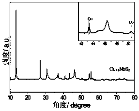
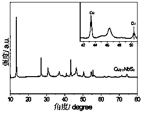
[0051] Preparation of 2D Cu x Nb 2 (0

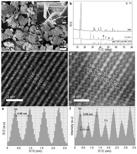
[0052] Step 1): take by weighing 0.67g metal Nb powder (purity ≥ 99.99%, particle diameter 325 orders) and 0.48g sublimated sulfur, in the glove box (H 2 O2 2 compound.

[0053] Step 2): Weigh 100.0mg NbS 2 and 2.0-80.9mg copper powder (purity ≥ 99.99%, particle size 1 μm), in a glove box full of Ar gas (H 2 O2 x Nb 2 (0

[0054] figure 1 Among (a) is the obtained NbS of the present embodiment 2 SEM image of the powder, NbS can be seen 2 is a typical two-dimensional layered material; figure 1 (b) is the XRD pattern obtained in this example, showing Cu and NbS 2 After the action, NbS 2 The (003) diffraction peaks of the NbS 2 The interlayer spacing increases, which may be caused by Cu atoms entering the interlayer. figure 1 (c) (d) (e) (f) is the NbS obtained in this embodiment 2 and Cu x Nb 2 The STEM image and...

Embodiment 2

[0057] Preparation of 2D Cu x TiS 2 The specific preparation method of the heterojunction material is as follows:

[0058] Step 1): Weigh 0.50g of metal Ti powder (purity ≥ 99.99%, particle size 325 mesh) and 0.69g of sublimated sulfur, in a glove box full of Ar gas (H 2 O2 2 compound.

[0059] Step 2): Weigh 100.0mg TiS 2 and 56.7mg of copper powder (purity ≥ 99.99%, particle size 1 μm), in a glove box full of Ar gas (H 2 O2 x TiS 2 heterojunction materials.

[0060] Figure 22 Among (a) is the obtained TiS of the present embodiment 2 SEM image of the powder, visible TiS 2 is a typical two-dimensional layered material; Figure 22 (b) is the XRD pattern obtained in this example, showing Cu and TiS 2 After the action, TiS 2 The (001) diffraction peaks of the TiS 2 The interlayer spacing increases, that is, Cu atoms enter the interlayer to form a two-dimensional heterojunction.

Embodiment 3

[0062] Preparation of 2D Cu x TT 2 The specific preparation method of the heterojunction material is as follows:

[0063] Step 1): take by weighing 0.50g metal Ta powder (purity ≥ 99.99%, particle diameter 325 orders) and 0.18g sublimated sulfur, in the glove box (H 2 O2 2 compound.

[0064] Step 2): Weigh 100.0mg TaS 2 and 25.9mg of copper powder (purity ≥ 99.99%, particle size 1μm), in a glove box full of Ar gas (H 2 O2 x TT 2 heterojunction materials.

[0065] Figure 23 Middle (a) is TaS obtained in the present embodiment 2 SEM image of powder, visible TaS 2 is a typical two-dimensional layered material; Figure 23(b) is the XRD pattern obtained in this example, showing Cu and TaS 2 After the action, TaS 2 The (001) diffraction peak of (001) is obviously shifted to a low angle, indicating that the interlayer spacing of TaS2 increases, that is, Cu atoms enter the interlayer to form a two-dimensional heterojunction.


PUM


Abstract

The invention discloses a novel two-dimensional heterojunction material and a preparation method thereof. The method for preparing a Cu intercalated TMDs compound is efficient and easy to operate, themethod can replace a traditional high-temperature solid-phase reaction, defects are prevented from being introduced into a TMDs bulk phase, the intercalation concentration of Cu can be accurately regulated and controlled, the maximum value can reach 1.2, and the obtained intercalated compound is uniform in property. The synthetic route of the heterojunction material is broadened, and the application potential of the two-dimensional conductor / semiconductor heterojunction material is explored.

Description

technical field [0001] The invention belongs to the field of heterojunction materials, and specifically refers to a novel two-dimensional heterojunction material and a preparation method thereof. Background technique [0002] Transition metal dichalcogenides (TMDs) have attracted extensive research interest due to their unique physical and chemical properties. In its hexagonal layered structure, each layer is covalently bonded to the chalcogen elements by metal atoms and sandwiched between the chalcogen elements, and the layers are stacked by van der Waals force. Due to the van der Waals force, the binding force between layers is weak, which provides the possibility for guest species (such as atoms, ions, inorganic and organic molecules) to intercalate between layers, and the intercalation of guest species changes the intrinsic properties of TMDs. nature of the symptoms. Specifically, guest species can tune the electronic structure of TMDs, leading to changes in the bandga...

Claims


Application Information

Patent Timeline
Patent Type & Authority Applications(China)
IPC IPC(8): C01G23/00C01G31/00C01G33/00C01G35/00C01B19/00B82Y30/00
CPCB82Y30/00C01B19/007C01G23/002C01G31/006C01G33/006C01G35/006C01P2002/72C01P2004/03C01P2004/64
Inventor 柯福生刘晓晨
Owner WUHAN UNIV
Why Eureka
Try Eureka