
LED chip packaging method and LED lamp bead

A technology of LED chips and LED lamp beads, which is applied in the direction of electrical components, circuits, semiconductor devices, etc., can solve the problems of inconsistent excitation efficiency and poor uniformity of light emission, and achieve the effect of reducing chromatic aberration, reducing the angle of light output, and uniform light output

Inactive Publication Date: 2020-05-15
SHENZHEN JUFEI OPTOELECTRONICS CO LTD
View PDF8 Cites 3 Cited by
  • Summary
  • Abstract
  • Description
  • Claims
  • Application Information

AI Technical Summary

Problems solved by technology

[0005] The LED chip packaging method and the LED lamp beads provided by the embodiments of the present invention mainly solve the technical problem of how to solve the problem of using a layer of fluorescent glue mixed with a variety of luminescence conversion media with inconsistent excitation efficiencies in the LED products in the prior art. layer, leading to the problem of poor uniformity of light emission of LED products

Method used


Image

  • LED chip packaging method and LED lamp bead
  • LED chip packaging method and LED lamp bead
  • LED chip packaging method and LED lamp bead

Examples


Embodiment 1

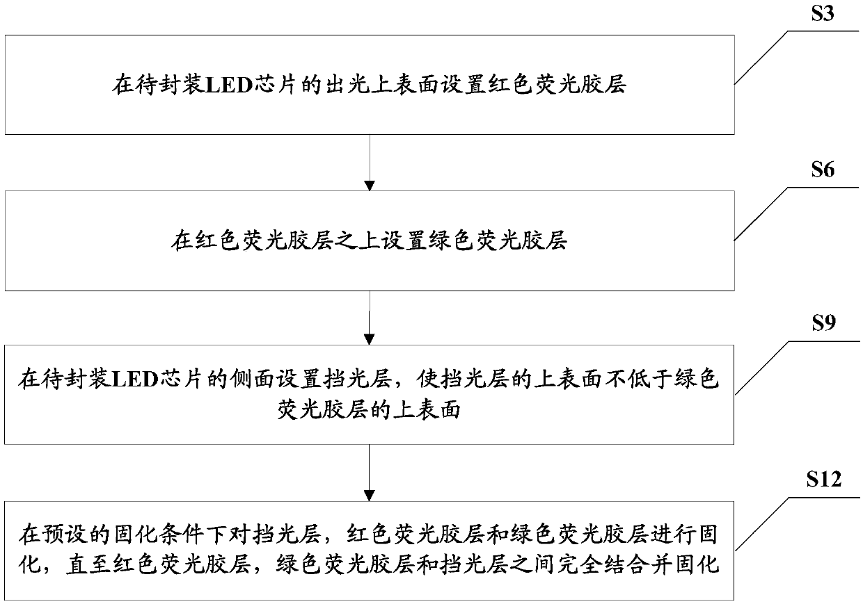
[0054] In order to solve the problem of poor luminous uniformity of LED products due to the installation of a layer of fluorescent adhesive layer mixed with various luminescence conversion media with inconsistent excitation efficiencies in the prior art, this embodiment provides a new LED chip package method, the LED lamp bead prepared by the LED chip encapsulation method emits light uniformly and has high luminous efficiency, please refer to the following image 3 The flow chart of the LED chip packaging method shown:

[0055] S3: setting a red fluorescent adhesive layer on the light emitting upper surface of the LED chip to be packaged.

[0056] S6: setting a green fluorescent glue layer on the red fluorescent glue layer.

[0057] It should be noted that, in some other embodiments, the positions of the red fluorescent glue layer and the green fluorescent glue layer can be interchanged, but preferably, the color segment with a larger wavelength should be set at the bottom, t...

Embodiment 2

[0076] It should be understood that the LED chip packaging method in this embodiment is applicable to the packaging of a single LED chip, and is also suitable for the packaging of LED chips in batches. An implementation process of batch encapsulation is taken as an example to illustrate below. For the encapsulation process see Figure 5 shown, including:

[0077] S501: Arranging at least two LED chips to be packaged on the preparation carrier according to a preset spacing distance.

[0078] Figure 6 It shows a schematic diagram of a preparation state for preparing wafer-level packaged LED lamp beads in batches. In this embodiment, the preparation carrier 62 is an auxiliary device for packaging LED chips 61 to obtain wafer-level packaged LED lamp beads, which is not a wafer-level packaged LED lamp bead. A part of encapsulating LED lamp beads. In an example of this embodiment, a high-temperature-resistant high-temperature film may be selected as the preparation carrier 62 i...

Embodiment 3

[0107] This embodiment provides an LED lamp bead, please refer to Figure 14 As shown, the LED lamp bead provided in this embodiment includes an LED chip 1401, a red fluorescent adhesive layer 1402, a green fluorescent adhesive layer 1403 and a light blocking layer 1404; wherein, preferably, a nitride red fluorescent adhesive layer can be used in this embodiment And nitride green fluorescent adhesive layer. Of course, in other embodiments, the fluorescent glue layer can also be made of a sulfide system or a silicate system. It should be understood that, in some other embodiments, the above-mentioned red fluorescent glue layer 1402 and green fluorescent glue layer 1403 may be replaced by colloid containing quantum dot photoluminescent material, or other luminescence conversion glue that can realize luminescence conversion. In the embodiment, the red fluorescent adhesive layer 1402 is located on the light emitting upper surface of the LED chip 1401, the green fluorescent adhesi...


PUM

PropertyMeasurementUnit
thicknessaaaaaaaaaa

Abstract

The invention provides an LED chip packaging method and an LED lamp bead. In the LED lamp bead prepared by the method, a red fluorescent glue layer and a green fluorescent glue layer are sequentiallyarranged on the light-emitting upper surface of the LED chip from bottom to top, so that the light emitted from the LED chip can be sequentially and uniformly converted in the two fluorescent glue layers, and finally, the LED lamp beads emit light more uniformly, the situations of color difference, yellow spots and the like can be reduced, and the light efficiency is improved. Besides, light blocking glue layers exist on the side faces of the LED chips in the LED lamp beads prepared through the method, the side face of the red fluorescent glue layer and the side face of the green fluorescent glue layer, and can block the light emitted by the LED chips, so that the light emitting angle can be reduced, and the LED lamp beads can be applied to more fields.

Description

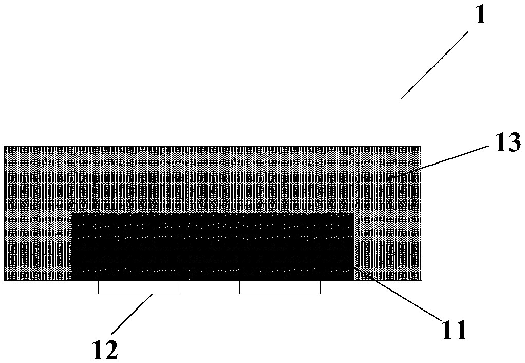
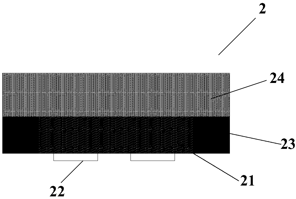
technical field [0001] The present invention relates to the field of LED (Light Emitting Diode, light emitting diode), in particular to an LED chip packaging method and an LED lamp bead. Background technique [0002] With the application and development of LEDs, the size requirements of LEDs are getting smaller and smaller. In order to meet the requirements of reducing the size of LEDs, chip-scale package CSP (Chip Scale Package, chip-level packaging) LEDs have emerged. The current CSP LEDs mainly have two structures: one is five-sided light-emitting CSP LEDs, and the CSP LEDs have The four sides and the top surface are light-emitting surfaces, and the bottom is provided with positive and negative electrodes. The other is a single-sided light-emitting CSP LED, which only has the top surface as the light-emitting surface, and its bottom surface is provided with positive and negative electrodes. [0003] figure 1 Shown is the most common five-sided light-emitting CSP LED la...

Claims


Application Information

Patent Timeline
Patent Type & Authority Applications(China)
IPC IPC(8): H01L33/58H01L33/50
CPCH01L33/504H01L33/58H01L2933/0041H01L2933/0058
Inventor 魏冬寒谭攀峰邢美正
Owner SHENZHEN JUFEI OPTOELECTRONICS CO LTD
Learn More