

TSV vacuum laminating method, apparatus, and bonding system using same
A vacuum layer and vacuum technology, which is applied in the manufacture of electrical components, electrical solid devices, semiconductor/solid devices, etc., can solve the problems of complex lamination, bonding and debonding processes, difficulty in maintenance, management and repair, and complex and large-scale devices and other problems, to achieve the effect of suppressing voids, saving maintenance and management costs, and simplifying process layout
- Summary
- Abstract
- Description
- Claims
- Application Information
AI Technical Summary
Problems solved by technology
Method used
Image

Examples
Embodiment Construction
[0036] The present invention relates to a lamination process of a through-silicon via (Through Silicon Via, hereinafter referred to as "TSV") process for improving the integration degree of semiconductor elements.
[0037] In particular, an adhesive film capable of efficiently laminating an adhesive film to a carrier wafer for maintaining the strength of a device wafer relates to a vacuum lamination for high-quality vacuum lamination capable of suppressing generation of dust and particles.
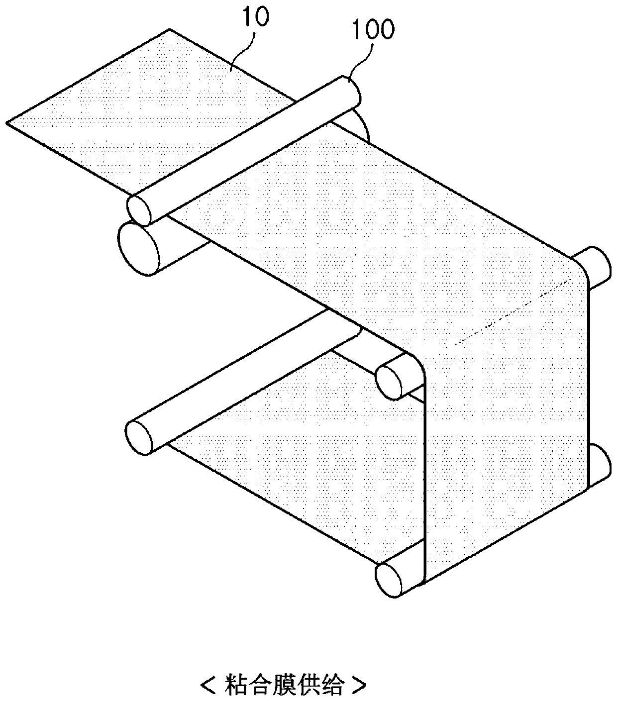
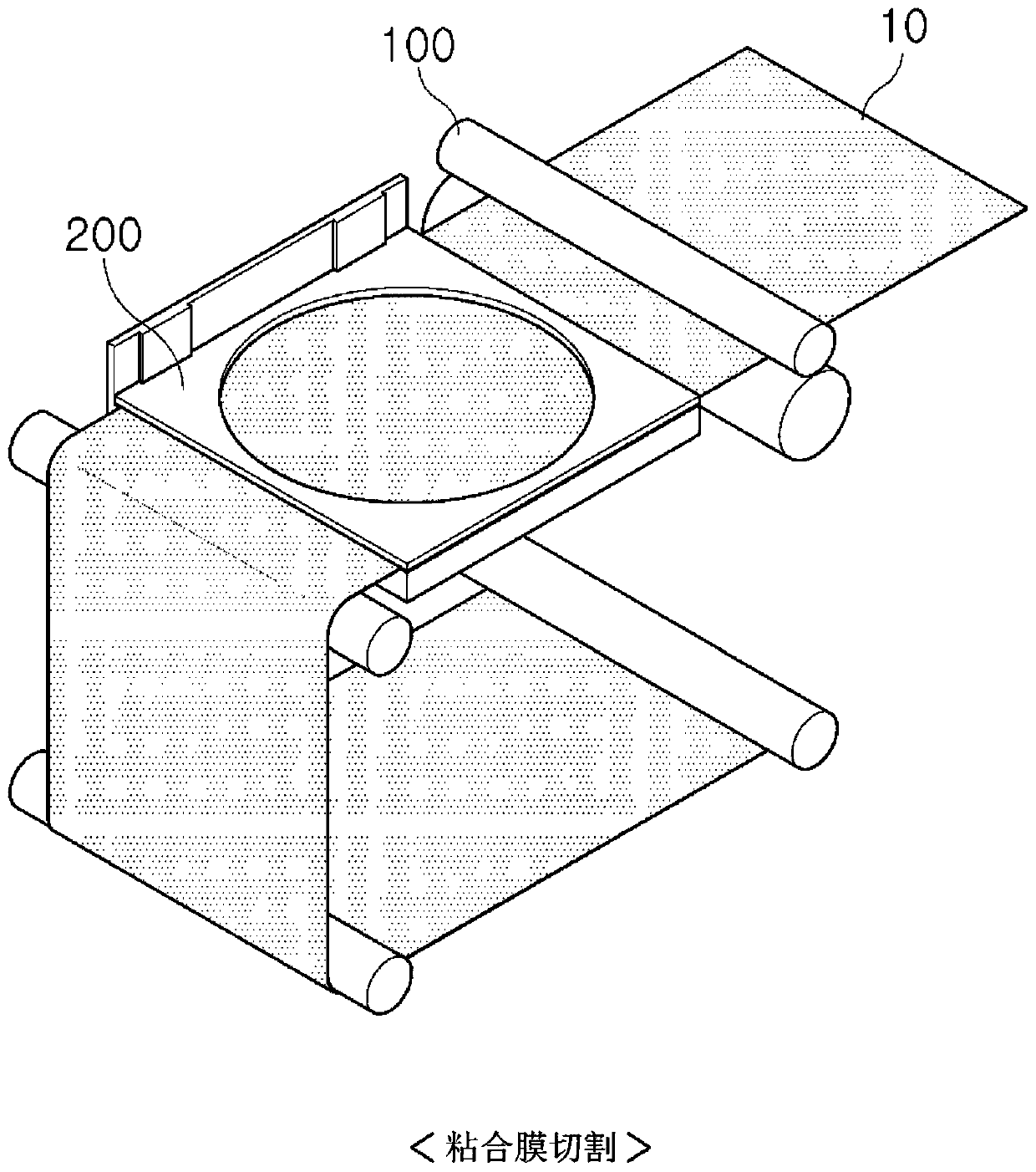
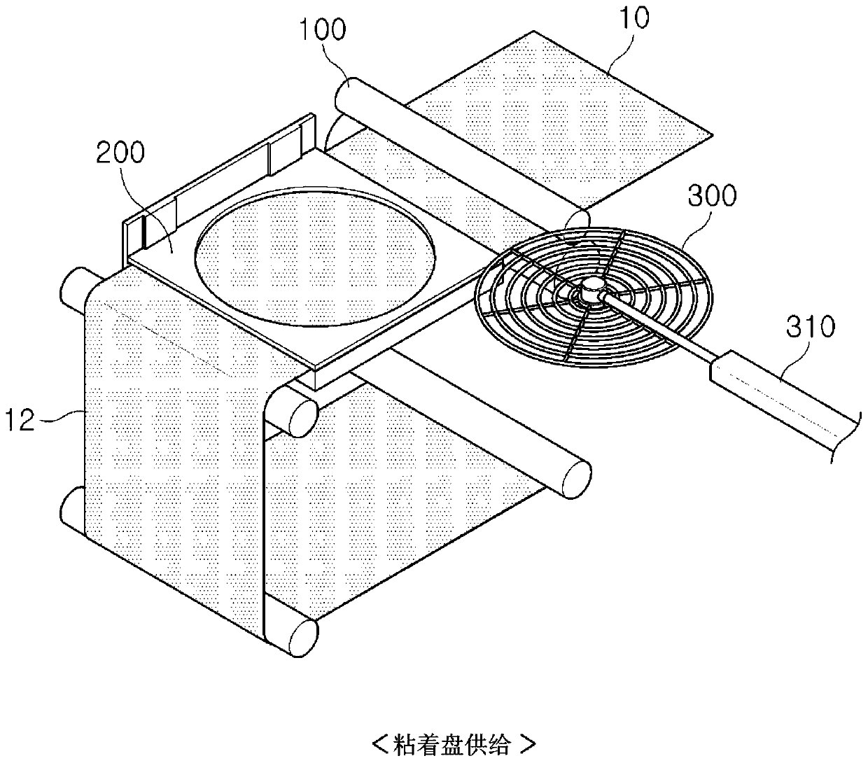
[0038] Figure 1 to Figure 8 is a schematic diagram of the vacuum lamination process sequence and the main parts of the device according to the present invention, Figure 9 to Figure 11 is a diagram illustrating an example of a bonding system according to vacuum lamination in the present invention.
[0039] As shown in the figure, in the present invention, the adhesive film 10 and the carrier wafer 20 are laminated in a vacuum state, so generation of dust and particles can be minimized, th...
PUM
 Abstract
Description
Claims
Application Information