Full GaN integrated half-bridge dead time adjusting circuit
A technology for adjusting circuit and dead time, applied in electrical components, high-efficiency power electronic conversion, output power conversion devices, etc., can solve problems such as increasing process difficulty and difficulty in designing full GaN digital circuits
- Summary
- Abstract
- Description
- Claims
- Application Information
AI Technical Summary
Problems solved by technology
Method used
Image
Examples
Embodiment approach
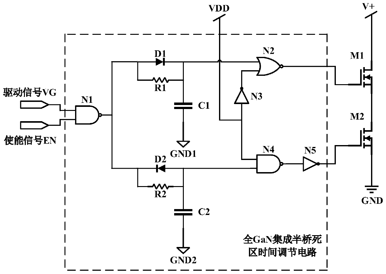
[0025] An embodiment of the present invention provides an all-GaN integrated half-bridge dead-time adjustment circuit, such as figure 1 As shown, it includes 2 NAND gate circuits N1 and N4, 1 NOR gate circuit N2, 2 NOT gate circuits N3 and N5, 2 diodes D1 and D2, 2 resistors R1 and R2, 2 capacitors C1 and C2.
[0026] The specific circuit structure has been described in detail in the content of the invention, and will not be repeated here.
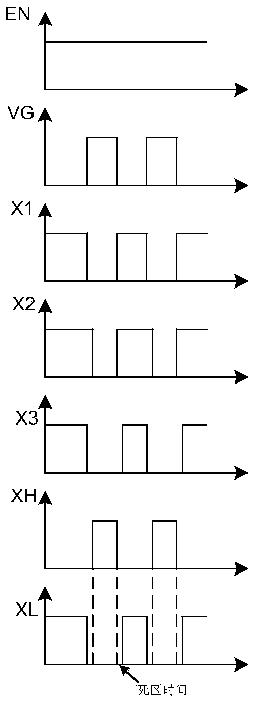
[0027] The working principle and process of the half-bridge circuit through protection circuit provided by the embodiment of the present invention will be described in detail below in conjunction with the accompanying drawings:
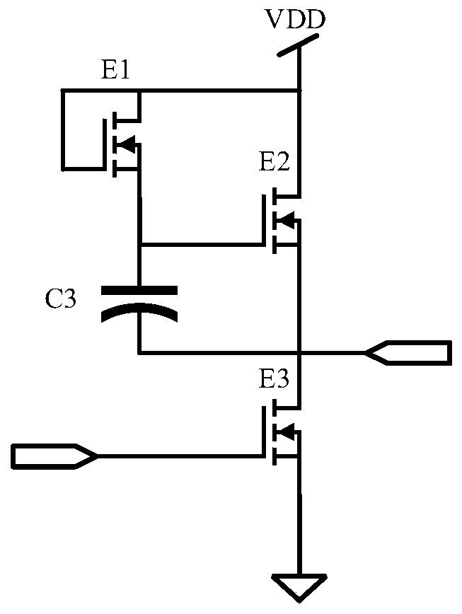
[0028] like image 3 As shown, the NOT gate circuit includes three transistors E1, E2 and E3, and one capacitor C3. When the voltage at the input terminal is low, the transistor E3 is in the off state, and the transistor E1 is in the on state because the gate and the drain are short-circuited, and the gate volt...
PUM
 Abstract
Description
Claims
Application Information


