Defect detection method and defect detection system

A defect detection and defect technology, applied in optical testing of defects/defects, measurement devices, material analysis by optical means, etc. The effect of reducing the number, reducing the time of scanning, increasing the capture capacity

Inactive Publication Date: 2020-05-22
SIEN QINGDAO INTEGRATED CIRCUITS CO LTD
View PDF0 Cites 0 Cited by
  • Summary
  • Abstract
  • Description
  • Claims
  • Application Information

AI Technical Summary

Problems solved by technology

[0003] In view of the above-mentioned shortcomings of the prior art, the object of the present invention is to provide a defect detection method and a defect detection system, which are used to solve the defects in the prior art that easily cause dark and bright areas to be missed. Problems with poor detection quality

Method used


Image

  • Defect detection method and defect detection system
  • Defect detection method and defect detection system
  • Defect detection method and defect detection system

Examples


Embodiment 1

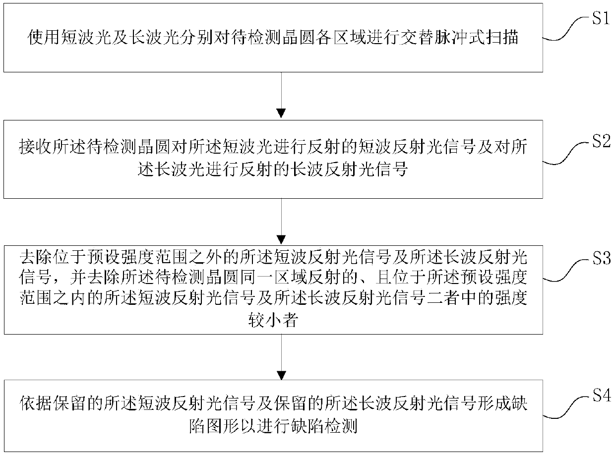
[0066] see figure 1 , the present invention provides a defect detection method, the defect detection method comprises the following steps:

[0067] 1) Use short-wavelength light and long-wavelength light to perform alternate pulse scanning on each area of ​​the wafer to be inspected;

[0068] 2) receiving a short-wave reflected light signal that reflects the short-wave light and a long-wave reflected light signal that reflects the long-wave light by the wafer to be detected;

[0069] 3) removing the short-wave reflected light signal and the long-wave reflected light signal outside the preset intensity range, and removing all light signals reflected from the same area of ​​the wafer to be inspected and within the preset intensity range The intensity of the short-wave reflected light signal and the long-wave reflected light signal is smaller;

[0070] 4) forming a defect pattern according to the retained short-wave reflected light signal and the retained long-wave reflected li...

Embodiment 2

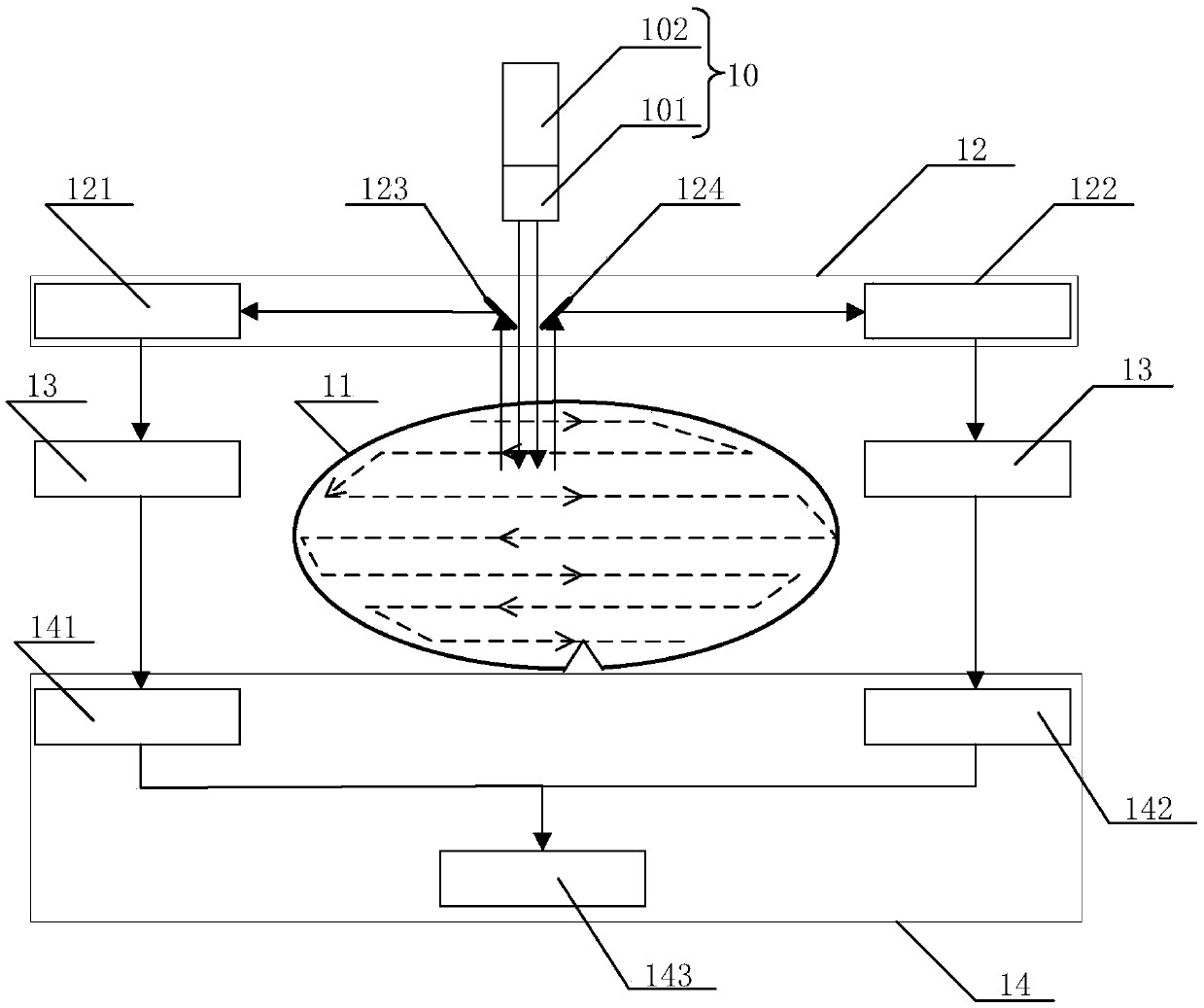
[0089] see figure 2 and image 3 The present invention also provides a defect detection system, which includes: a light source device 10, a detection device 12, a comparison processing device 13, and an imaging detection device 14; wherein, the light source device 10 is located on the wafer 11 to be detected above, the light source device 10 includes a short-wave light source 101 and a long-wave light source 102, and the light source device 10 is used to alternately emit short-wave light and long-wave light to perform alternate pulse scanning on each area of ​​the wafer 11 to be inspected, that is The short-wave light source 101 and the long-wave light source 102 alternately emit corresponding light; the detection device 12 is located on the upper side of the wafer 11 to be inspected, and the detection device 12 is used to receive the wafer 11 to be inspected The short-wave reflected light signal that reflects the short-wave light and the long-wave reflected light signal tha...


PUM

PropertyMeasurementUnit
wavelengthaaaaaaaaaa

Abstract

The invention provides a defect detection method and a defect detection system. The defect detection method comprises the following steps: 1) respectively carrying out alternate pulse type scanning oneach region of a wafer to be detected by using short-wave light and long-wave light; 2) receiving a short-wave reflected light signal of the wafer to be detected for reflecting the short-wave light and a long-wave reflected light signal of the wafer to be detected for reflecting the long-wave light; 3) removing the short-wave reflected light signal and the long-wave reflected light signal which are located outside the preset intensity range, and removing the lower-intensity one of the short-wave reflected light signal and the long-wave reflected light signal which are reflected in the same area of the wafer to be detected and located within the preset intensity range; and 4) forming a defect pattern according to the reserved short-wave reflected light signal and the reserved long-wave reflected light signal so as to perform defect detection. The brightness optimization of each area can be ensured, the defect capturing capability can be improved and the missing detection of defects canbe avoided.

Description

technical field [0001] The invention belongs to the technical field of semiconductors, and in particular relates to a defect detection method and a defect detection system. Background technique [0002] In the wafer manufacturing process, the light source used for defect detection is generally a light source with a fixed wavelength, but the care area in the defect detection process is generally divided into SRAM (static random access memory) by function ), logic (logic area) and full chip area (full die), the brightness and darkness of these areas vary greatly under the same beam of light source, especially some high-end flash memory (Flash) products, the characteristics of these products are The aspect ratio of the pattern (pattern) in the device cell (CELL) area is very large (can exceed 40:1), but this area is the core part of the flash memory product, and the bottom of the device cell area (belonging to the dark area) requires a higher Sensitivity and a short-wavelength...

Claims


Application Information

Patent Timeline
Patent Type & Authority Applications(China)
IPC IPC(8): G01N21/95
CPCG01N21/9501
Inventor 王通许继仁林庆儒
Owner SIEN QINGDAO INTEGRATED CIRCUITS CO LTD
Why Eureka
Try Eureka